KiCad automation tool for documents generation

Project description
KiBot (formerly KiPlot)


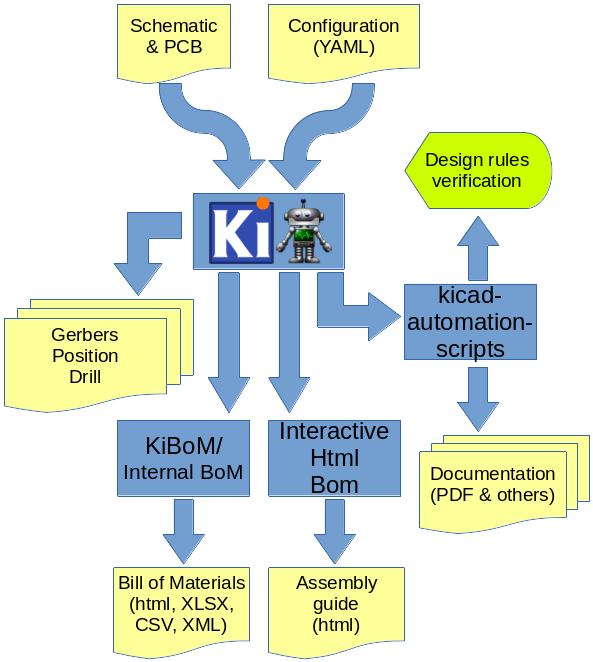
KiBot is a program which helps you to generate the fabrication and documentation files for your KiCad projects easily, repeatable, and most of all, scriptably. This means you can use a Makefile to export your KiCad PCBs just as needed.
For example, it's common that you might want for each board rev:
- Check ERC/DRC one last time (using KiCad Automation Scripts)
- Gerbers, drills and drill maps for a fab in their favourite format
- Fab docs for the assembler, including the BoM (Bill of Materials)
- Pick and place files
- PCB 3D model in STEP format
You want to do this in a one-touch way, and make sure everything you need to do so it securely saved in version control, not on the back of an old datasheet.
KiBot lets you do this. The following picture depicts the data flow:
The configuration file
KiBot uses a configuration file where you can specify what outputs to generate. By default you'll generate all of them, but you can specify which ones from the command line.
The configuration file should be named using the .kibot.yaml suffix, i.e. my_project.kibot.yaml. The format used is YAML. This is basically a text file with some structure. This file can be compressed using gzip file format.
If you never used YAML read the following explanation. Note that the explanation could be useful even if you know YAML.
The header
All configuration files must start with:
kibot:
  version: 1
This tells to KiBot that this file is using version 1 of the format.
The preflight section
This section is used to specify tasks that will be executed before generating any output.
Supported preflight options:
- check_zone_fills: [boolean=false] Zones are filled before doing any operation involving PCB layers.
- filters: [list(dict)] A list of entries to filter out ERC/DRC messages.
- Valid keys:
- error_number: Alias for number.
filter: [string=''] Name for the filter, for documentation purposes.- filter_msg: Alias for filter.
number: [number=0] Error number we want to exclude.regex: [string='None'] Regular expression to match the text for the error we want to exclude.- regexp: Alias for regex.
- Valid keys:
- ignore_unconnected: [boolean=false] Option for
run_drc. Ignores the unconnected nets. Useful if you didn't finish the routing. - run_drc: [boolean=false] Runs the DRC (Distance Rules Check). To ensure we have a valid PCB.
- run_erc: [boolean=false] Runs the ERC (Electrical Rules Check). To ensure the schematic is electrically correct.
- update_xml: [boolean=false] Update the XML version of the BoM (Bill of Materials).
To ensure our generated BoM is up to date.
Note that this isn't needed when using the internal BoM generator (
bom).
Here is an example of a preflight section:
preflight:
  run_erc: true
  update_xml: true
  run_drc: true
  check_zone_fills: true
  ignore_unconnected: false
Filtering DRC/ERC errors
Sometimes KiCad reports DRC or ERC errors that you can't get rid off. This could be just because you are part of a team including lazzy people that doesn't want to take the extra effort to solve some errors that aren't in fact errors, just small violations made on purpose. In this case you could exclude some known errors.
For this you must declare filters entry in the preflight section. Then you can add as many filter entries as you want.
Each filter entry has an optional description and defines to which error type is applied (number) and a regular expression
that the error must match to be ignored (regex). Like this:
  filters:
    - filter: 'Optional filter description'
      number: Numeric_error_type
      regex:  'Expression to match'
Here is an example, suppose you are getting the following errors:
** Found 1 DRC errors **
ErrType(4): Track too close to pad
    @(177.185 mm, 78.315 mm): Track 1.000 mm [Net-(C3-Pad1)] on F.Cu, length: 1.591 mm
    @(177.185 mm, 80.715 mm): Pad 2 of C3 on F.Cu and others

** Found 1 unconnected pads **
ErrType(2): Unconnected items
    @(177.185 mm, 73.965 mm): Pad 2 of C4 on F.Cu and others
    @(177.185 mm, 80.715 mm): Pad 2 of C3 on F.Cu and others
And you want to ignore them. You can add the following filters:
  filters:
    - filter: 'Ignore C3 pad 2 too close to anything'
      number: 4
      regex:  'Pad 2 of C3'
    - filter: 'Ignore unconnected pad 2 of C4'
      number: 2
      regex:  'Pad 2 of C4'
If you need to match text from two different lines in the error message try using (?s)TEXT(.*)TEXT_IN_OTHER_LINE.
If you have two or more different options for a text to match try using (OPTION1|OPTION2).
A complete Python regular expressions explanation is out the scope of this manual. For a complete reference consult the Python manual.
Important note: this will create a file named kibot_errors.filter in the output directory.
Default global options
The section global contains default global options that affects all the outputs.
Currently only one option is supported.
Default output option
This option controls the default file name pattern used by all the outputs. This makes all the file names coherent. You can always choose the file name for a particular output.
The pattern uses the following expansions:
- %f original pcb/sch file name without extension.
- %p pcb/sch title from pcb metadata.
- %c company from pcb/sch metadata.
- %r revision from pcb/sch metadata.
- %d pcb/sch date from metadata if available, file modification date otherwise.
- %D date the script was started.
- %T time the script was started.
- %i a contextual ID, depends on the output type.
- %x a suitable extension for the output type.
They are compatible with the ones used by IBoM.
The default value for global.output is %f-%i.%x.
If you want to include the revision you could add the following definition:
global:
  output: '%f_rev_%r-%i.%x'
The outputs section
In this section you put all the things that you want to generate. This section contains one or more outputs. Each output contain the following data:
namea name so you can easily identify it.commenta short description of this output.typeselects which type of output will be generated. Examples are gerbers, drill files and pick & place filesdiris the directory where this output will be stored.optionscontains one or more options to configure this output.layersa list of layers used for this output. Not all outputs needs this subsection.
Important note about the layers: In the original kiplot (from John Beard) the name of the inner layers was Inner.N where N is the number of the layer, i.e. Inner.1 is the first inner layer. This format is supported for compatibility. Note that this generated a lot of confusion because the default KiCad name for the first inner layer is In1.Cu. People filled issues and submitted pull-requests to fix it, thinking that inner layers weren't supported. Currently KiCad allows renaming these layers, so this version of kiplot supports the name used in KiCad. Just use the same name you see in the user interface.
The available values for type are:
- Plot formats:
gerberthe gerbers for fabrication.pspostscript plothpglformat for laser printerssvgscalable vector graphicspdfportable document formatdxfmechanical CAD format
- Drill formats:
excellondata for the drilling machinegerb_drilldrilling positions in a gerber file
- Pick & place
positionof the components for the pick & place machine
- Documentation
pdf_sch_printschematic in PDF formatpdf_pcb_printPDF file containing one or more layer and the page frame
- Bill of Materials
kibomBoM in HTML or CSV format generated by KiBoMibomInteractive HTML BoM generated by InteractiveHtmlBom
- 3D model:
stepStandard for the Exchange of Product Data for the PCB
Here is an example of a configuration file to generate the gerbers for the top and bottom layers:
kibot:
  version: 1

preflight:
  run_drc: true

outputs:

  - name: 'gerbers'
    comment: "Gerbers for the board house"
    type: gerber
    dir: gerberdir
    options:
      # generic layer options
      exclude_edge_layer: false
      exclude_pads_from_silkscreen: false
      plot_sheet_reference: false
      plot_footprint_refs: true
      plot_footprint_values: true
      force_plot_invisible_refs_vals: false
      tent_vias: true
      line_width: 0.15

      # gerber options
      use_aux_axis_as_origin: false
      subtract_mask_from_silk: true
      use_protel_extensions: false
      gerber_precision: 4.5
      create_gerber_job_file: true
      use_gerber_x2_attributes: true
      use_gerber_net_attributes: false

    layers:
      - 'F.Cu'
      - 'B.Cu'
Most options are the same you'll find in the KiCad dialogs.
Specifying the layers
You have various ways to specify the layers. If you need to specify just one layer you can just use its name:
layers: 'F.Cu'
If you want to specify all the available layers:
layers: 'all'
You can also select the layers you want in KiCad (using File, Plot dialog) and save your PCB. Then you just need to use:
layers: 'selected'
You can also use any of the following grup of layers:
- copper all the copper layers
- technical all the technical layers (silk sreen, solder mask, paste, adhesive, etc.)
- user all the user layers (draw, comments, eco, margin, edge cuts, etc.)
You can also mix the above definitions using a list:
    layers:
      - 'copper'
      - 'Dwgs.User'
This will select all the copper layers and the user drawings. Note that the above mentioned options will use file name suffixes and descriptions selected automatically. If you want to use a particular suffix and provide better descriptions you can use the following format:
    layers:
      - layer: 'F.Cu'
        suffix: 'F_Cu'
        description: 'Front copper'
      - layer: 'B.Cu'
        suffix: 'B_Cu'
        description: 'Bottom copper'
You can also mix the styles:
    layers:
      - 'copper'
      - layer: 'Cmts.User'
        suffix: 'Cmts_User'
        description: 'User comments'
      - 'Dwgs.User'
If you need to use the same list of layers for various outputs you can use YAML anchors. The first time you define the list of layers just assign an ancho, here is an example:
    layers: &copper_and_cmts
      - copper
      - 'Cmts.User'
Next time you need this list just use an alias, like this:
layers: *copper_and_cmts
Supported outputs:
-
BoM (Bill of Materials)
- Type:
bom - Description: Used to generate the BoM in CSV, HTML, TSV, TXT, XML or XLSX format using the internal BoM.
Is compatible with KiBoM, but doesn't need to update the XML netlist because the components
are loaded from the schematic.
Important differences with KiBoM output:
- All options are in the main
optionssection, not inconfsubsection. - TheComponentcolumn is namedRowand works just like any other column. This output is what you get from the 'Tools/Generate Bill of Materials' menu in eeschema. - Valid keys:
comment: [string=''] A comment for documentation purposes.dir: [string='.'] Output directory for the generated files.name: [string=''] Used to identify this particular output definition.options: [dict] Options for thebomoutput.- Valid keys:
columns: [list(dict)|list(string)] List of columns to display. Can be just the name of the field.- Valid keys:
field: [string=''] Name of the field to use for this column.join: [list(string)|string=''] List of fields to join to this column.name: [string=''] Name to display in the header. The field is used when empty.
- Valid keys:
component_aliases: [list(list(string))] A series of values which are considered to be equivalent for the part name. Each entry is a list of equivalen names. Example: ['c', 'c_small', 'cap' ] will ensure the equivalent capacitor symbols can be grouped together. If empty the following aliases are used: - ['r', 'r_small', 'res', 'resistor'] - ['l', 'l_small', 'inductor'] - ['c', 'c_small', 'cap', 'capacitor'] - ['sw', 'switch'] - ['zener', 'zenersmall'] - ['d', 'diode', 'd_small'].csv: [dict] Options for the CSV, TXT and TSV formats.- Valid keys:
hide_pcb_info: [boolean=false] Hide project information.hide_stats_info: [boolean=false] Hide statistics information.quote_all: [boolean=false] Enclose all values using double quotes.separator: [string=','] CSV Separator. TXT and TSV always use tab as delimiter.
- Valid keys:
exclude_any: [list(dict)] A series of regular expressions used to exclude parts. If a component matches ANY of these, it will be excluded. Column names are case-insensitive. If empty the following list is used: - column: References regex: '^TP[0-9]*' - column: References regex: '^FID' - column: Part regex: 'mount.*hole' - column: Part regex: 'solder.*bridge' - column: Part regex: 'solder.*jump' - column: Part regex: 'test.*point' - column: Footprint regex: 'test.*point' - column: Footprint regex: 'mount.*hole' - column: Footprint regex: 'fiducial'.- Valid keys:
column: [string=''] Name of the column to apply the regular expression.- field: Alias for column.
regex: [string=''] Regular expression to match.- regexp: Alias for regex.
- Valid keys:
fit_field: [string='Config'] Field name used to determine if a particular part is to be fitted (also DNC and variants).format: [string=''] [HTML,CSV,TXT,TSV,XML,XLSX] format for the BoM. If empty defaults to CSV or a guess according to the options..group_connectors: [boolean=true] Connectors with the same footprints will be grouped together, independent of the name of the connector.group_fields: [list(string)] List of fields used for sorting individual components into groups. Components which match (comparing all fields) will be grouped together. Field names are case-insensitive. If empty: ['Part', 'Part Lib', 'Value', 'Footprint', 'Footprint Lib'] is used.html: [dict] Options for the HTML format.- Valid keys:
col_colors: [boolean=true] Use colors to show the field type.datasheet_as_link: [string=''] Column with links to the datasheet.digikey_link: [string|list(string)=''] Column/s containing Digi-Key part numbers, will be linked to web page.generate_dnf: [boolean=true] Generate a separated section for DNF (Do Not Fit) components.hide_pcb_info: [boolean=false] Hide project information.hide_stats_info: [boolean=false] Hide statistics information.highlight_empty: [boolean=true] Use a color for empty cells. Applies only whencol_colorsistrue.logo: [string|boolean=''] PNG file to use as logo, use false to remove.style: [string='modern-blue'] Page style. Internal styles: modern-blue, modern-green, modern-red and classic. Or you can provide a CSS file name. Please use .css as file extension..title: [string='KiBot Bill of Materials'] BoM title.
- Valid keys:
ignore_dnf: [boolean=true] Exclude DNF (Do Not Fit) components.include_only: [list(dict)] A series of regular expressions used to select included parts. If there are any regex defined here, only components that match against ANY of them will be included. Column names are case-insensitive. If empty all the components are included.- Valid keys:
column: [string=''] Name of the column to apply the regular expression.- field: Alias for column.
regex: [string=''] Regular expression to match.- regexp: Alias for regex.
- Valid keys:
merge_blank_fields: [boolean=true] Component groups with blank fields will be merged into the most compatible group, where possible.normalize_locale: [boolean=false] When normalizing values use the locale decimal point.normalize_values: [boolean=false] Try to normalize the R, L and C values, producing uniform units and prefixes.number: [number=1] Number of boards to build (components multiplier).output: [string='%f-%i.%x'] filename for the output (%i=bom). Affected by global options.test_regex: [boolean=true] Each component group will be tested against a number of regular-expressions (seeinclude_onlyandexclude_any).use_alt: [boolean=false] Print grouped references in the alternate compressed style eg: R1-R7,R18.variant: [string|list(string)=''] Board variant(s), used to determine which components are output to the BoM..xlsx: [dict] Options for the XLSX format.- Valid keys:
col_colors: [boolean=true] Use colors to show the field type.datasheet_as_link: [string=''] Column with links to the datasheet.digikey_link: [string|list(string)=''] Column/s containing Digi-Key part numbers, will be linked to web page.generate_dnf: [boolean=true] Generate a separated section for DNF (Do Not Fit) components.hide_pcb_info: [boolean=false] Hide project information.hide_stats_info: [boolean=false] Hide statistics information.highlight_empty: [boolean=true] Use a color for empty cells. Applies only whencol_colorsistrue.logo: [string|boolean=''] PNG file to use as logo, use false to remove.max_col_width: [number=60] [20,999] Maximum column width (characters).style: [string='modern-blue'] Head style: modern-blue, modern-green, modern-red and classic..title: [string='KiBot Bill of Materials'] BoM title.
- Valid keys:
- Valid keys:
- Type:
-
DXF (Drawing Exchange Format)
- Type:
dxf - Description: Exports the PCB to 2D mechanical EDA tools (like AutoCAD). This output is what you get from the File/Plot menu in pcbnew.
- Valid keys:
comment: [string=''] A comment for documentation purposes.dir: [string='.'] Output directory for the generated files.layers: [list(dict)|list(string)|string] [all,selected,copper,technical,user] List of PCB layers to plot.- Valid keys:
description: [string=''] A description for the layer, for documentation purposes.layer: [string=''] Name of the layer. As you see it in KiCad.suffix: [string=''] Suffix used in file names related to this layer. Derived from the name if not specified.
- Valid keys:
name: [string=''] Used to identify this particular output definition.options: [dict] Options for thedxfoutput.- Valid keys:
drill_marks: [string='full'] what to use to indicate the drill places, can be none, small or full (for real scale).exclude_edge_layer: [boolean=true] do not include the PCB edge layer.exclude_pads_from_silkscreen: [boolean=false] do not plot the component pads in the silk screen.force_plot_invisible_refs_vals: [boolean=false] include references and values even when they are marked as invisible.metric_units: [boolean=false] use mm instead of inches.output: [string='%f-%i.%x'] output file name, the default KiCad name if empty. Affected by global options.plot_footprint_refs: [boolean=true] include the footprint references.plot_footprint_values: [boolean=true] include the footprint values.plot_sheet_reference: [boolean=false] currently without effect.polygon_mode: [boolean=true] plot using the contour, instead of the center line.sketch_plot: [boolean=false] don't fill objects, just draw the outline.tent_vias: [boolean=true] cover the vias.use_aux_axis_as_origin: [boolean=false] use the auxiliar axis as origin for coordinates.
- Valid keys:
- Type:
-
Excellon drill format
- Type:
excellon - Description: This is the main format for the drilling machine. You can create a map file for documentation purposes. This output is what you get from the 'File/Fabrication output/Drill Files' menu in pcbnew.
- Valid keys:
comment: [string=''] A comment for documentation purposes.dir: [string='.'] Output directory for the generated files.name: [string=''] Used to identify this particular output definition.options: [dict] Options for theexcellonoutput.- Valid keys:
map: [dict|string] [hpgl,ps,gerber,dxf,svg,pdf] format for a graphical drill map. Not generated unless a format is specified.- Valid keys:
output: [string='%f-%i.%x'] name for the map file, KiCad defaults if empty (%i='PTH_drill_map'). Affected by global options.type: [string='pdf'] [hpgl,ps,gerber,dxf,svg,pdf] format for a graphical drill map.
- Valid keys:
metric_units: [boolean=true] use metric units instead of inches.minimal_header: [boolean=false] use a minimal header in the file.mirror_y_axis: [boolean=false] invert the Y axis.output: [string='%f-%i.%x'] name for the drill file, KiCad defaults if empty (%i='PTH_drill'). Affected by global options.pth_and_npth_single_file: [boolean=true] generate one file for both, plated holes and non-plated holes, instead of two separated files.report: [dict|string] name of the drill report. Not generated unless a name is specified.- Valid keys:
filename: [string=''] name of the drill report. Not generated unless a name is specified. (%i='drill_report' %x='txt').
- Valid keys:
use_aux_axis_as_origin: [boolean=false] use the auxiliar axis as origin for coordinates.
- Valid keys:
- Type:
-
Gerber drill format
- Type:
gerb_drill - Description: This is the information for the drilling machine in gerber format. You can create a map file for documentation purposes. This output is what you get from the 'File/Fabrication output/Drill Files' menu in pcbnew.
- Valid keys:
comment: [string=''] A comment for documentation purposes.dir: [string='.'] Output directory for the generated files.name: [string=''] Used to identify this particular output definition.options: [dict] Options for thegerb_drilloutput.- Valid keys:
map: [dict|string] [hpgl,ps,gerber,dxf,svg,pdf] format for a graphical drill map. Not generated unless a format is specified.- Valid keys:
output: [string='%f-%i.%x'] name for the map file, KiCad defaults if empty (%i='PTH_drill_map'). Affected by global options.type: [string='pdf'] [hpgl,ps,gerber,dxf,svg,pdf] format for a graphical drill map.
- Valid keys:
output: [string='%f-%i.%x'] name for the drill file, KiCad defaults if empty (%i='PTH_drill'). Affected by global options.report: [dict|string] name of the drill report. Not generated unless a name is specified.- Valid keys:
filename: [string=''] name of the drill report. Not generated unless a name is specified. (%i='drill_report' %x='txt').
- Valid keys:
use_aux_axis_as_origin: [boolean=false] use the auxiliar axis as origin for coordinates.
- Valid keys:
- Type:
-
Gerber format
- Type:
gerber - Description: This is the main fabrication format for the PCB. This output is what you get from the File/Plot menu in pcbnew.
- Valid keys:
comment: [string=''] A comment for documentation purposes.dir: [string='.'] Output directory for the generated files.layers: [list(dict)|list(string)|string] [all,selected,copper,technical,user] List of PCB layers to plot.- Valid keys:
description: [string=''] A description for the layer, for documentation purposes.layer: [string=''] Name of the layer. As you see it in KiCad.suffix: [string=''] Suffix used in file names related to this layer. Derived from the name if not specified.
- Valid keys:
name: [string=''] Used to identify this particular output definition.options: [dict] Options for thegerberoutput.- Valid keys:
create_gerber_job_file: [boolean=true] creates a file with information about all the generated gerbers. You can use it in gerbview to load all gerbers at once.exclude_edge_layer: [boolean=true] do not include the PCB edge layer.exclude_pads_from_silkscreen: [boolean=false] do not plot the component pads in the silk screen.force_plot_invisible_refs_vals: [boolean=false] include references and values even when they are marked as invisible.gerber_job_file: [string='%f-%i.%x'] name for the gerber job file (%i='job', %x='gbrjob').gerber_precision: [number=4.6] this the gerber coordinate format, can be 4.5 or 4.6.line_width: [number=0.1] [0.02,2] line_width for objects without width [mm].output: [string='%f-%i.%x'] output file name, the default KiCad name if empty. Affected by global options.plot_footprint_refs: [boolean=true] include the footprint references.plot_footprint_values: [boolean=true] include the footprint values.plot_sheet_reference: [boolean=false] currently without effect.subtract_mask_from_silk: [boolean=false] substract the solder mask from the silk screen.tent_vias: [boolean=true] cover the vias.use_aux_axis_as_origin: [boolean=false] use the auxiliar axis as origin for coordinates.use_gerber_net_attributes: [boolean=true] include netlist metadata.use_gerber_x2_attributes: [boolean=true] use the extended X2 format.use_protel_extensions: [boolean=false] use legacy Protel file extensions.
- Valid keys:
- Type:
-
HPGL (Hewlett & Packard Graphics Language)
- Type:
hpgl - Description: Exports the PCB for plotters and laser printers. This output is what you get from the File/Plot menu in pcbnew.
- Valid keys:
comment: [string=''] A comment for documentation purposes.dir: [string='.'] Output directory for the generated files.layers: [list(dict)|list(string)|string] [all,selected,copper,technical,user] List of PCB layers to plot.- Valid keys:
description: [string=''] A description for the layer, for documentation purposes.layer: [string=''] Name of the layer. As you see it in KiCad.suffix: [string=''] Suffix used in file names related to this layer. Derived from the name if not specified.
- Valid keys:
name: [string=''] Used to identify this particular output definition.options: [dict] Options for thehpgloutput.- Valid keys:
drill_marks: [string='full'] what to use to indicate the drill places, can be none, small or full (for real scale).exclude_edge_layer: [boolean=true] do not include the PCB edge layer.exclude_pads_from_silkscreen: [boolean=false] do not plot the component pads in the silk screen.force_plot_invisible_refs_vals: [boolean=false] include references and values even when they are marked as invisible.mirror_plot: [boolean=false] plot mirrored.output: [string='%f-%i.%x'] output file name, the default KiCad name if empty. Affected by global options.pen_number: [number=1] [1,16] pen number.pen_speed: [number=20] [1,99] pen speed.pen_width: [number=15] [0,100] pen diameter in MILS, useful to fill areas. However, it is in mm in HPGL files.plot_footprint_refs: [boolean=true] include the footprint references.plot_footprint_values: [boolean=true] include the footprint values.plot_sheet_reference: [boolean=false] currently without effect.scaling: [number=0] scale factor (0 means autoscaling).sketch_plot: [boolean=false] don't fill objects, just draw the outline.tent_vias: [boolean=true] cover the vias.
- Valid keys:
- Type:
-
IBoM (Interactive HTML BoM)
- Type:
ibom - Description: Generates an interactive web page useful to identify the position of the components in the PCB. For more information: https://github.com/INTI-CMNB/InteractiveHtmlBom This output is what you get from the InteractiveHtmlBom plug-in (pcbnew).
- Valid keys:
comment: [string=''] A comment for documentation purposes.dir: [string='.'] Output directory for the generated files.name: [string=''] Used to identify this particular output definition.options: [dict] Options for theibomoutput.- Valid keys:
blacklist: [string=''] List of comma separated blacklisted components or prefixes with . E.g. 'X1,MH'.blacklist_empty_val: [boolean=false] Blacklist components with empty value.board_rotation: [number=0] Board rotation in degrees (-180 to 180). Will be rounded to multiple of 5.bom_view: [string='left-right'] [bom-only,left-right,top-bottom] Default BOM view.checkboxes: [string='Sourced,Placed'] Comma separated list of checkbox columns.dark_mode: [boolean=false] Default to dark mode.dnp_field: [string=''] Name of the extra field that indicates do not populate status. Components with this field not empty will be blacklisted.extra_fields: [string=''] Comma separated list of extra fields to pull from netlist or xml file.hide_pads: [boolean=false] Hide footprint pads by default.hide_silkscreen: [boolean=false] Hide silkscreen by default.highlight_pin1: [boolean=false] Highlight pin1 by default.include_nets: [boolean=false] Include netlist information in output..include_tracks: [boolean=false] Include track/zone information in output. F.Cu and B.Cu layers only.layer_view: [string='FB'] [F,FB,B] Default layer view.name_format: [string='ibom'] Output file name format supports substitutions: %f : original pcb file name without extension. %p : pcb/project title from pcb metadata. %c : company from pcb metadata. %r : revision from pcb metadata. %d : pcb date from metadata if available, file modification date otherwise. %D : bom generation date. %T : bom generation time. Extension .html will be added automatically. Note that this name is used only when output is ''.netlist_file: [string=''] Path to netlist or xml file.no_blacklist_virtual: [boolean=false] Do not blacklist virtual components.no_redraw_on_drag: [boolean=false] Do not redraw pcb on drag by default.normalize_field_case: [boolean=false] Normalize extra field name case. E.g. 'MPN' and 'mpn' will be considered the same field.output: [string='%f-%i.%x'] Filename for the output, use '' to use the IBoM filename (%i=ibom, %x=html). Affected by global options.show_fabrication: [boolean=false] Show fabrication layer by default.sort_order: [string='C,R,L,D,U,Y,X,F,SW,A,,HS,CNN,J,P,NT,MH'] Default sort order for components. Must contain '' once.variant_field: [string=''] Name of the extra field that stores board variant for component.variants_blacklist: [string=''] List of board variants to exclude from the BOM.variants_whitelist: [string=''] List of board variants to include in the BOM.
- Valid keys:
- Type:
-
KiBoM (KiCad Bill of Materials)
- Type:
kibom - Description: Used to generate the BoM in HTML or CSV format using the KiBoM plug-in. For more information: https://github.com/INTI-CMNB/KiBoM This output is what you get from the 'Tools/Generate Bill of Materials' menu in eeschema.
- Valid keys:
comment: [string=''] A comment for documentation purposes.dir: [string='.'] Output directory for the generated files.name: [string=''] Used to identify this particular output definition.options: [dict] Options for thekibomoutput.- Valid keys:
conf: [string|dict] BoM configuration file, relative to PCB. You can also define the configuration here, will be stored inconfig.kibom.ini.- Valid keys:
columns: [list(dict)|list(string)] List of columns to display. Can be just the name of the field.- Valid keys:
field: [string=''] Name of the field to use for this column.join: [list(string)|string=''] List of fields to join to this column.name: [string=''] Name to display in the header. The field is used when empty.
- Valid keys:
component_aliases: [list(list(string))] A series of values which are considered to be equivalent for the part name. Each entry is a list of equivalen names. Example: ['c', 'c_small', 'cap' ] will ensure the equivalent capacitor symbols can be grouped together. If empty the following aliases are used: - ['r', 'r_small', 'res', 'resistor'] - ['l', 'l_small', 'inductor'] - ['c', 'c_small', 'cap', 'capacitor'] - ['sw', 'switch'] - ['zener', 'zenersmall'] - ['d', 'diode', 'd_small'].datasheet_as_link: [string=''] Column with links to the datasheet (HTML only).digikey_link: [string|list(string)=''] Column/s containing Digi-Key part numbers, will be linked to web page (HTML only).exclude_any: [list(dict)] A series of regular expressions used to exclude parts. If a component matches ANY of these, it will be excluded. Column names are case-insensitive. If empty the following list is used: - column: References regex: '^TP[0-9]*' - column: References regex: '^FID' - column: Part regex: 'mount.*hole' - column: Part regex: 'solder.*bridge' - column: Part regex: 'test.*point' - column: Footprint regex 'test.*point' - column: Footprint regex: 'mount.*hole' - column: Footprint regex: 'fiducial'.- Valid keys:
column: [string=''] Name of the column to apply the regular expression.- field: Alias for column.
regex: [string=''] Regular expression to match.- regexp: Alias for regex.
- Valid keys:
fit_field: [string='Config'] Field name used to determine if a particular part is to be fitted (also DNC and variants).group_connectors: [boolean=true] Connectors with the same footprints will be grouped together, independent of the name of the connector.group_fields: [list(string)] List of fields used for sorting individual components into groups. Components which match (comparing all fields) will be grouped together. Field names are case-insensitive. If empty: ['Part', 'Part Lib', 'Value', 'Footprint', 'Footprint Lib'] is used.hide_headers: [boolean=false] Hide column headers.hide_pcb_info: [boolean=false] Hide project information.html_generate_dnf: [boolean=true] Generate a separated section for DNF (Do Not Fit) components (HTML only).ignore_dnf: [boolean=true] Exclude DNF (Do Not Fit) components.include_only: [list(dict)] A series of regular expressions used to select included parts. If there are any regex defined here, only components that match against ANY of them will be included. Column names are case-insensitive. If empty all the components are included.- Valid keys:
column: [string=''] Name of the column to apply the regular expression.- field: Alias for column.
regex: [string=''] Regular expression to match.- regexp: Alias for regex.
- Valid keys:
merge_blank_fields: [boolean=true] Component groups with blank fields will be merged into the most compatible group, where possible.number_rows: [boolean=true] First column is the row number.test_regex: [boolean=true] Each component group will be tested against a number of regular-expressions (see ``)..use_alt: [boolean=false] Print grouped references in the alternate compressed style eg: R1-R7,R18.
- Valid keys:
format: [string='HTML'] [HTML,CSV,XML,XLSX] format for the BoM.number: [number=1] Number of boards to build (components multiplier).output: [string='%f-%i.%x'] filename for the output (%i=bom). Affected by global options.separator: [string=','] CSV Separator.variant: [string=''] Board variant(s), used to determine which components are output to the BoM. To specify multiple variants, with a BOM file exported for each variant, separate variants with the ';' (semicolon) character.
- Valid keys:
- Type:
-
PcbDraw - Beautiful 2D PCB render
- Type:
pcbdraw - Description: Exports the PCB as a 2D model (SVG, PNG or JPG). Uses configurable colors. Can also render the components if the 2D models are available
- Valid keys:
comment: [string=''] A comment for documentation purposes.dir: [string='.'] Output directory for the generated files.name: [string=''] Used to identify this particular output definition.options: [dict] Options for thepcbdrawoutput.- Valid keys:
bottom: [boolean=false] render the bottom side of the board (default is top side).dpi: [number=300] [10,1200] dots per inch (resolution) of the generated image.format: [string='svg'] [svg,png,jpg] output format. Only used if nooutputis specified.highlight: [list(string)=[]] list of components to highlight.libs: [list(string)=[]] list of libraries.mirror: [boolean=false] mirror the board.no_drillholes: [boolean=false] do not make holes transparent.output: [string='%f-%i.%x'] name for the generated file. Affected by global options.placeholder: [boolean=false] show placeholder for missing components.remap: [dict|None] replacements for PCB references using components (lib:component).show_components: [string|list(string)=none] [none,all] list of components to draw, can be also a string for none or all. The default is none.style: [string|dict] PCB style (colors). An internal name, the name of a JSON file or the style options.- Valid keys:
board: [string='#4ca06c'] color for the board without copper (covered by solder mask).clad: [string='#9c6b28'] color for the PCB core (not covered by solder mask).copper: [string='#417e5a'] color for the copper zones (covered by solder mask).highlight_on_top: [boolean=false] highlight over the component (not under).highlight_padding: [number=1.5] [0,1000] how much the highlight extends around the component [mm].highlight_style: [string='stroke:none;fill:#ff0000;opacity:0.5;'] SVG code for the highlight style.outline: [string='#000000'] color for the outline.pads: [string='#b5ae30'] color for the exposed pads (metal finish).silk: [string='#f0f0f0'] color for the silk screen.vcut: [string='#bf2600'] color for the V-CUTS.
- Valid keys:
vcuts: [boolean=false] render V-CUTS on the Cmts.User layer.warnings: [string='visible'] [visible,all,none] using visible only the warnings about components in the visible side are generated.
- Valid keys:
- Type:
-
PDF (Portable Document Format)
- Type:
pdf - Description: Exports the PCB to the most common exhange format. Suitable for printing. Note that this output isn't the best for documating your project. This output is what you get from the File/Plot menu in pcbnew.
- Valid keys:
comment: [string=''] A comment for documentation purposes.dir: [string='.'] Output directory for the generated files.drill_marks: [string='full'] what to use to indicate the drill places, can be none, small or full (for real scale).exclude_edge_layer: [boolean=true] do not include the PCB edge layer.exclude_pads_from_silkscreen: [boolean=false] do not plot the component pads in the silk screen.force_plot_invisible_refs_vals: [boolean=false] include references and values even when they are marked as invisible.layers: [list(dict)|list(string)|string] [all,selected,copper,technical,user] List of PCB layers to plot.- Valid keys:
description: [string=''] A description for the layer, for documentation purposes.layer: [string=''] Name of the layer. As you see it in KiCad.suffix: [string=''] Suffix used in file names related to this layer. Derived from the name if not specified.
- Valid keys:
name: [string=''] Used to identify this particular output definition.options: [dict] Options for thepdfoutput.- Valid keys:
drill_marks: [string='full'] what to use to indicate the drill places, can be none, small or full (for real scale).exclude_edge_layer: [boolean=true] do not include the PCB edge layer.exclude_pads_from_silkscreen: [boolean=false] do not plot the component pads in the silk screen.force_plot_invisible_refs_vals: [boolean=false] include references and values even when they are marked as invisible.line_width: [number=0.1] [0.02,2] for objects without width [mm].mirror_plot: [boolean=false] plot mirrored.negative_plot: [boolean=false] invert black and white.output: [string='%f-%i.%x'] output file name, the default KiCad name if empty. Affected by global options.plot_footprint_refs: [boolean=true] include the footprint references.plot_footprint_values: [boolean=true] include the footprint values.plot_sheet_reference: [boolean=false] currently without effect.tent_vias: [boolean=true] cover the vias.
- Valid keys:
output: [string='%f-%i.%x'] output file name, the default KiCad name if empty. Affected by global options.plot_footprint_refs: [boolean=true] include the footprint references.plot_footprint_values: [boolean=true] include the footprint values.plot_sheet_reference: [boolean=false] currently without effect.tent_vias: [boolean=true] cover the vias.
- Type:
-
PDF PCB Print (Portable Document Format)
- Type:
pdf_pcb_print - Description: Exports the PCB to the most common exhange format. Suitable for printing. This is the main format to document your PCB. This output is what you get from the 'File/Print' menu in pcbnew.
- Valid keys:
comment: [string=''] A comment for documentation purposes.dir: [string='.'] Output directory for the generated files.layers: [list(dict)|list(string)|string] [all,selected,copper,technical,user] List of PCB layers to include in the PDF.- Valid keys:
description: [string=''] A description for the layer, for documentation purposes.layer: [string=''] Name of the layer. As you see it in KiCad.suffix: [string=''] Suffix used in file names related to this layer. Derived from the name if not specified.
- Valid keys:
name: [string=''] Used to identify this particular output definition.options: [dict] Options for thepdf_pcb_printoutput.- Valid keys:
output: [string='%f-%i.%x'] filename for the output PDF (%i=layers, %x=pdf). Affected by global options.- output_name: Alias for output.
- Valid keys:
- Type:
-
PDF Schematic Print (Portable Document Format)
- Type:
pdf_sch_print - Description: Exports the PCB to the most common exhange format. Suitable for printing. This is the main format to document your schematic. This output is what you get from the 'File/Print' menu in eeschema.
- Valid keys:
comment: [string=''] A comment for documentation purposes.dir: [string='.'] Output directory for the generated files.name: [string=''] Used to identify this particular output definition.options: [dict] Options for thepdf_sch_printoutput.- Valid keys:
output: [string='%f-%i.%x'] filename for the output PDF (%i=schematic %x=pdf). Affected by global options.
- Valid keys:
- Type:
-
Pick & place
- Type:
position - Description: Generates the file with position information for the PCB components, used by the pick and place machine. This output is what you get from the 'File/Fabrication output/Footprint poistion (.pos) file' menu in pcbnew.
- Valid keys:
comment: [string=''] A comment for documentation purposes.dir: [string='.'] Output directory for the generated files.name: [string=''] Used to identify this particular output definition.options: [dict] Options for thepositionoutput.- Valid keys:
format: [string='ASCII'] [ASCII,CSV] format for the position file.only_smd: [boolean=true] only include the surface mount components.output: [string='%f-%i.%x'] output file name (%i='top_pos'|'bottom_pos'|'both_pos', %x='pos'|'csv'). Affected by global options.separate_files_for_front_and_back: [boolean=true] generate two separated files, one for the top and another for the bottom.units: [string='millimeters'] [millimeters,inches] units used for the positions.
- Valid keys:
- Type:
-
PS (Postscript)
- Type:
ps - Description: Exports the PCB to a format suitable for printing. This output is what you get from the File/Plot menu in pcbnew.
- Valid keys:
comment: [string=''] A comment for documentation purposes.dir: [string='.'] Output directory for the generated files.layers: [list(dict)|list(string)|string] [all,selected,copper,technical,user] List of PCB layers to plot.- Valid keys:
description: [string=''] A description for the layer, for documentation purposes.layer: [string=''] Name of the layer. As you see it in KiCad.suffix: [string=''] Suffix used in file names related to this layer. Derived from the name if not specified.
- Valid keys:
name: [string=''] Used to identify this particular output definition.options: [dict] Options for thepsoutput.- Valid keys:
a4_output: [boolean=true] force A4 paper size.drill_marks: [string='full'] what to use to indicate the drill places, can be none, small or full (for real scale).exclude_edge_layer: [boolean=true] do not include the PCB edge layer.exclude_pads_from_silkscreen: [boolean=false] do not plot the component pads in the silk screen.force_plot_invisible_refs_vals: [boolean=false] include references and values even when they are marked as invisible.line_width: [number=0.15] [0.02,2] for objects without width [mm].mirror_plot: [boolean=false] plot mirrored.negative_plot: [boolean=false] invert black and white.output: [string='%f-%i.%x'] output file name, the default KiCad name if empty. Affected by global options.plot_footprint_refs: [boolean=true] include the footprint references.plot_footprint_values: [boolean=true] include the footprint values.plot_sheet_reference: [boolean=false] currently without effect.scale_adjust_x: [number=1.0] fine grain adjust for the X scale (floating point multiplier).scale_adjust_y: [number=1.0] fine grain adjust for the Y scale (floating point multiplier).scaling: [number=1] scale factor (0 means autoscaling).sketch_plot: [boolean=false] don't fill objects, just draw the outline.tent_vias: [boolean=true] cover the vias.width_adjust: [number=0] this width factor is intended to compensate PS printers/plotters that do not strictly obey line width settings. Only used to plot pads and tracks.
- Valid keys:
- Type:
-
STEP (ISO 10303-21 Clear Text Encoding of the Exchange Structure)
- Type:
step - Description: Exports the PCB as a 3D model. This is the most common 3D format for exchange purposes. This output is what you get from the 'File/Export/STEP' menu in pcbnew.
- Valid keys:
comment: [string=''] A comment for documentation purposes.dir: [string='.'] Output directory for the generated files.name: [string=''] Used to identify this particular output definition.options: [dict] Options for thestepoutput.- Valid keys:
metric_units: [boolean=true] use metric units instead of inches.min_distance: [number=-1] the minimum distance between points to treat them as separate ones (-1 is KiCad default: 0.01 mm).no_virtual: [boolean=false] used to exclude 3D models for components with 'virtual' attribute.origin: [string='grid'] determines the coordinates origin. Using grid the coordinates are the same as you have in the design sheet. The drill option uses the auxiliar reference defined by the user. You can define any other origin using the format 'X,Y', i.e. '3.2,-10'.output: [string='%f-%i.%x'] name for the generated STEP file (%i='3D' %x='step'). Affected by global options.
- Valid keys:
- Type:
-
SVG (Scalable Vector Graphics)
- Type:
svg - Description: Exports the PCB to a format suitable for 2D graphics software. Unlike bitmaps SVG drawings can be scaled without losing resolution. This output is what you get from the File/Plot menu in pcbnew.
- Valid keys:
comment: [string=''] A comment for documentation purposes.dir: [string='.'] Output directory for the generated files.layers: [list(dict)|list(string)|string] [all,selected,copper,technical,user] List of PCB layers to plot.- Valid keys:
description: [string=''] A description for the layer, for documentation purposes.layer: [string=''] Name of the layer. As you see it in KiCad.suffix: [string=''] Suffix used in file names related to this layer. Derived from the name if not specified.
- Valid keys:
name: [string=''] Used to identify this particular output definition.options: [dict] Options for thesvgoutput.- Valid keys:
drill_marks: [string='full'] what to use to indicate the drill places, can be none, small or full (for real scale).exclude_edge_layer: [boolean=true] do not include the PCB edge layer.exclude_pads_from_silkscreen: [boolean=false] do not plot the component pads in the silk screen.force_plot_invisible_refs_vals: [boolean=false] include references and values even when they are marked as invisible.line_width: [number=0.25] [0.02,2] for objects without width [mm].mirror_plot: [boolean=false] plot mirrored.negative_plot: [boolean=false] invert black and white.output: [string='%f-%i.%x'] output file name, the default KiCad name if empty. Affected by global options.plot_footprint_refs: [boolean=true] include the footprint references.plot_footprint_values: [boolean=true] include the footprint values.plot_sheet_reference: [boolean=false] currently without effect.tent_vias: [boolean=true] cover the vias.
- Valid keys:
- Type:
-
SVG Schematic Print
- Type:
svg_sch_print - Description: Exports the PCB. Suitable for printing. This is a format to document your schematic.
- Valid keys:
comment: [string=''] A comment for documentation purposes.dir: [string='.'] Output directory for the generated files.name: [string=''] Used to identify this particular output definition.options: [dict] Options for thesvg_sch_printoutput.- Valid keys:
output: [string='%f-%i.%x'] filename for the output SVG (%i=schematic %x=svg). Affected by global options.
- Valid keys:
- Type:
Using KiBot
If you need a template for the configuration file try:
kibot --example
This will generate a file named example.kibot.yaml containing all the available options and comments about them.
You can use it to create your own configuration file.
If you want to use the layers of a particular PCB in the example use:
kibot -b PCB_FILE --example
And if you want to use the same options selected in the plot dialog use:
kibot -b PCB_FILE -p --example
If the current directory contains only one PCB file and only one configuration file (named *.kibot.yaml)
you can just call kibot. No arguments needed. The tool will figure out which files to use.
If more than one file is found in the current directory kibot will use the first found and issue a
warning. If you need to use other file just tell it explicitly:
kibot -b PCB_FILE.kicad_pcb -c CONFIG.kibot.yaml
A simple target can be added to your makefile, so you can just run
make pcb_files or integrate into your current build process.
pcb_files:
    kibot -b $(PCB) -c $(KIBOT_CFG)
If you need to supress messages use --quiet or -q and if you need to get more informatio about
what's going on use --verbose or -v.
If you want to generate only some of the outputs use:
kibot OUTPUT_1 OUTPUT_2
If you want to generate all outputs with some exceptions use:
kibot --invert-sel OUTPUT_1 OUTPUT_2
If you want to skip the DRC and ERC use:
kibot --skip-pre run_erc,run_drc
If you want to skip all the preflight tasks use:
kibot --skip-pre all
All outputs are generated using the current directory as base. If you want to use another directory as base use:
kibot --out-dir OTHER_PLACE
If you want to list the available outputs defined in the configuration file use:
kibot --list
Command line help
KiBot: KiCad automation tool for documents generation

Usage:
  kibot [-b BOARD] [-e SCHEMA] [-c CONFIG] [-d OUT_DIR] [-s PRE]
         [-q | -v...] [-i] [TARGET...]
  kibot [-v...] [-c PLOT_CONFIG] --list
  kibot [-v...] [-b BOARD] [-d OUT_DIR] [-p | -P] --example
  kibot [-v...] --help-list-outputs
  kibot [-v...] --help-output=HELP_OUTPUT
  kibot [-v...] --help-outputs
  kibot [-v...] --help-preflights
  kibot -h | --help
  kibot --version

Arguments:
  TARGET    Outputs to generate, default is all

Options:
  -h, --help                       Show this help message and exit
  -b BOARD, --board-file BOARD     The PCB .kicad-pcb board file
  -c CONFIG, --plot-config CONFIG  The plotting config file to use
  -d OUT_DIR, --out-dir OUT_DIR    The output directory [default: .]
  -e SCHEMA, --schematic SCHEMA    The schematic file (.sch)
  --help-list-outputs              List supported outputs
  --help-output HELP_OUTPUT        Help for this particular output
  --help-outputs                   List supported outputs and details
  --help-preflights                List supported preflights and details
  -i, --invert-sel                 Generate the outputs not listed as targets
  -l, --list                       List available outputs (in the config file)
  -p, --copy-options               Copy plot options from the PCB file
  -P, --copy-and-expand            As -p but expand the list of layers
  -q, --quiet                      Remove information logs
  -s PRE, --skip-pre PRE           Skip preflights, comma separated or `all`
  -v, --verbose                    Show debugging information
  -V, --version                    Show program's version number and exit
  -x, --example                    Create an example configuration file.
Installing
Dependencies
- For ERC, DRC, BoM XML update and PCB/SCH print install KiCad Automation Scripts
- BoM files (HTML/CSV/TSV/TXT/XML/XLSX) can be generated using the internal BoM generator or using KiBoM.
- For interactive BoM install InteractiveHtmlBom
- For SVG/PNG/JPG beauty PCB render PcbDraw
Installation on Ubuntu/Debian:
Get the Debian package from the releases section and run:
sudo apt install ./kibot*_all.deb
Important note: Sometimes the release needs another packages that aren't part of the stable Debian distribution. In this case the packages are also included in the release page. As an example version 0.6.0 needs:
sudo apt install ./python3-mcpy_2.0.2-1_all.deb ./kibot_0.6.0-1_all.deb
Installation using pip:
pip install --no-compile kibot
Note that pip has the dubious idea of compiling everything it downloads.
There is no advantage in doing it and it interferes with the mcpy macros.
Installation on other targets
- Install KiCad 5.x
- Install Python 3.5 or newer
- Install the Python Yaml module
- Run the script src/kibot
Using for CI/CD
When using a GitHub or GitLab repo you can use KiBot to generate all the needed stuff each time you commit a change to the schematic and/or PCB file.
Examples of how to do it can be found here for GitHub and here for GitLab.
In order to run KiBot on these environments you need a lot of software installed. The usual mechanism to achieve this is using docker. Docker images containing KiBot, all the supporting scripts and a corresponding KiCad can be found at Docker Hub as setsoft/kicad_auto:latest. This image is based on setsoft/kicad_debian:latest, containing KiCad on Debian GNU/Linux.
For more information about the docker images visit kicad_debian and kicad_auto.
Credits
- KiBot project: Salvador E. Tropea (@set-soft)
- Original KiPlot project: John Beard (@johnbeard)
- Original KiCad Automation Scripts: Scott Bezek, Productize SPRL
- KiBoM: Oliver Henry Walters (@SchrodingersGat)
- Interactive HTML BoM: @qu1ck
- PcbDraw: Jan Mrázek (@yaqwsx)
- Contributors:
- Error filters ideas: Leandro Heck (@leoheck)
- SVG output: @nerdyscout
- Others:
- Robot in the logo: Christian Plaza (from pixabay)
Release history Release notifications | RSS feed


Download files
Download the file for your platform. If you're not sure which to choose, learn more about installing packages.
Source Distribution
Built Distribution
Filter files by name, interpreter, ABI, and platform.
If you're not sure about the file name format, learn more about wheel file names.
Copy a direct link to the current filters
File details
Details for the file kibot-0.6.2.tar.gz.
File metadata
- Download URL: kibot-0.6.2.tar.gz
- Upload date:
- Size: 170.2 kB
- Tags: Source
- Uploaded using Trusted Publishing? No
- Uploaded via: twine/1.13.0 pkginfo/1.4.2 requests/2.21.0 setuptools/40.8.0 requests-toolbelt/0.8.0 tqdm/4.28.1 CPython/3.7.3
File hashes
| Algorithm | Hash digest | |
|---|---|---|
| SHA256 |
d7e86f228cb1b9a20ab2f95e6d77e01035d073d42bc8c883aa7dbc2b7adc814f
|
|
| MD5 |
42365967d3f4f80e28aad80d0fb5e56d
|
|
| BLAKE2b-256 |
cc11369ba3f0d6d0d1941b346cbfba7932300df001afdebbd2f6ab029e87be4f
|
File details
Details for the file kibot-0.6.2-py3-none-any.whl.
File metadata
- Download URL: kibot-0.6.2-py3-none-any.whl
- Upload date:
- Size: 174.8 kB
- Tags: Python 3
- Uploaded using Trusted Publishing? No
- Uploaded via: twine/1.13.0 pkginfo/1.4.2 requests/2.21.0 setuptools/40.8.0 requests-toolbelt/0.8.0 tqdm/4.28.1 CPython/3.7.3
File hashes
| Algorithm | Hash digest | |
|---|---|---|
| SHA256 |
f01aedba109339c7a1bb1af4b9deae48b014b6bb5de480aec3f84ff259149845
|
|
| MD5 |
110dea5eecfc913ea922d4538d825968
|
|
| BLAKE2b-256 |
f6660c9d5622a4d2f52f0a069cd913b64d0de47a390fbaed93c0c121d3e1cf4d
|