A friendly way to skip the drudgery and manipulate kicad 7+ s-expression schematic, netlist and PCB files

Project description
kicad skip: S-expression kicad file python parser
Copyright © 2024 Pat Deegan, psychogenic.com
This library lets you manipulate kicad schematic (and other) source files with Python, simply.
At a minimum it presents a usable interface to the s-expression structure to add or modify data, but it also does a lot behind the scenes to make both scripting and exploration using the REPL shell efficient and enjoyable.
Main features
-
Explore, modify and create elements of a schematic or PCB using Python
-
Access to every bit of the source file using a common API
-
Kicad-specific enhancements to allow for
- searching for elements by location, by connection (things that are attached to other things via wires), by type...
- search for symbols by name or regex, on reference or value
- easily access the location of any symbol pin, and more
-
Lots of REPL-friendly features, so you can see at a glance what an element is, access it by name (e.g. schematic.symbol.R14.dnp), use TAB-completion
Overview and Walk-through video
I've put out an intro video where I walk through some REPL usage and create a LED array generator. To see that click on:

I've also put up a Scripting For Kicad Schematics In Python blog post, with some intro, background and hopefully more human-friendly reading.
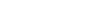
Explore the schematic or PCB
You can load a schematic or PCB in a Python shell, and the system provides facilities to easily traverse and inspect the elements.
Above is a sample of interaction with a schematic. The same holds true for PCBs (.kicad_pcb files), though to date less effort has been put towards enhancing basic functions (but see the PCB section below).
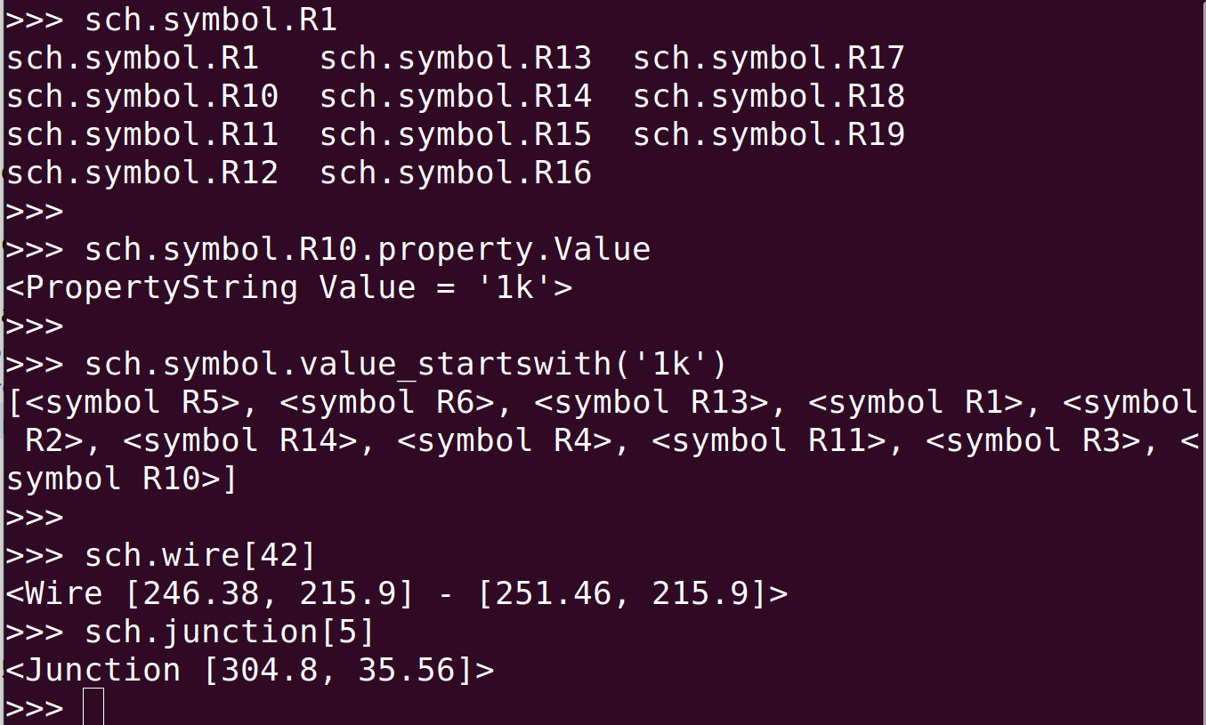
Script away drudgery
This array of LEDs
was created, wired up and labelled with a short script, available in an example. The example now provides for both XY grid and charlieplexed arrays, and shows how to clone elements, wire things up, and play with both types of label.
I did a quick walk-through demo live on the maker cast, and it starts exactly here, in MakerCast episode 56
Motivation
Kicad schematic, layout and other files are stored as trees of s-expressions, like
(kicad_sch (version 20230121) (generator eeschema)
  (uuid 20adca1d-43a1-4784-9682-8b7dd1c7d330)
  (title_block (title "My Demo Board") (date "2024-01-31") (rev "1.0.5")
    (company "Psychogenic Technologies") (comment 1 "(C) 2023, 2024 Pat Deegan")
  )
  (lib_symbols
    (symbol "74xx:74CBTLV3257" (in_bom yes) (on_board yes)
      (property "Reference" "U" (at 17.78 1.27 0) (effects (font (size 1.27 1.27))))
      (property "Value" "74CBTLV3257" (at 15.24 -1.27 0)(effects (font (size 1.27 1.27))))
  ...
  (symbol (lib_id "SomeLib:Partname") (at 317.5 45.72 0) (unit 1)
    (in_bom yes) (on_board yes) (dnp no)
    (uuid 342c76f3-b2b8-40b2-a0b0-d83e480188cc)
    (property "Reference" "J4" (at 311.15 29.21 0)(effects (font (size 1.27 1.27))))
    (property "Value" "TT04_BREAKOUT_REVB" (at 317.5 76.2 0) (effects (font (size 1.27 1.27))))
    (pin "A10" (uuid bf1f9b27-0b93-4778-ac69-684e16bea09c))
  ...
which are great for machine parsing, but not so much for a quick scripted manipulation.
Though you can use the lib to quickly explore and modify the contents of any s-expression file, skip is optimized for use with kicad schematics (eeschema kicad_sch files), with some enhanced support for important elements of PCB layout files as well.
Examples
Effort has been made to make exploring the contents easy. This means:
named attributes
Where possible, collections have named attributes: do use TAB-completion, schem. etc
Examples
>>> schem.symbol.U TAB TAB
outputs (something like, depending on schematic):
  schem.symbol.U1    schem.symbol.U3      schem.symbol.U4_B    schem.symbol.U4_D
  schem.symbol.U2    schem.symbol.U4_A    schem.symbol.U4_C    schem.symbol.U4_E
and
>>> schem.symbol.U1.property. TAB TAB
outputs
 schem.symbol.U1.property.Characteristics
 schem.symbol.U1.property.Datasheet
 schem.symbol.U1.property.DigikeyPN
 schem.symbol.U1.property.Footprint
 schem.symbol.U1.property.MPN
 schem.symbol.U1.property.Reference
 schem.symbol.U1.property.Value
representation
__repr__ and __str__ overrides so you have an idea what you're looking at. Just enter the variable in the REPL console and it should spit something sane out.
>>> schem
<Schematic 'samp/my_schematic.kicad_sch'>

>>> schem.symbol[23]
<symbol C28>

>>> schem.symbol[23].property
<Collection [<PropertyString Reference = 'C28'>,
 <PropertyString Value = '100nF'>,
 <PropertyString Footprint = 'Capacitor_SMD:C_0402_1005Metric'>,
 <PropertyString Datasheet = '~'>, <PropertyString JLC = ''>,
 <PropertyString Part_number = ''>, <PropertyString MPN = 'CL05A104KA5NNNC'>,
 <PropertyString Characteristics = '100n 10% 25V XR 0402'>,
 <PropertyString MPN_ALT = 'GRM155R71E104KE14J'>]>

>>> schem.wire[22]
<Wire [314.96, 152.4] - [317.5, 152.4]>

>>> schem.text[4]
<text 'Options fo...'>

# and much more, e.g. for library symbols, junctions, labels, whatever's in there
Quick walkthrough
Here's some sample interaction with the library. The basic functions allow you to view and edit attributes. More involved helpers let you search and crawl the schematic to find things.
basic
# load a schematic
schem = skip.Schematic('samp/my_schem.kicad_sch')

# loop over all components, treat collection as array
for component in schem.symbol:
    component # do something

# search through the symbols by reference or value, using regex or starts_with
>>> schem.symbol.reference_matches(r'(C|R)2[158]')
[<symbol C25>, <symbol C28>, <symbol R25>, <symbol C21>,
 <symbol R21>, <symbol R28>]

>>> sorted(schem.symbol.value_startswith('10k'))
[<symbol R12>, <symbol R30>, <symbol R31>, <symbol R32>, <symbol R33>,
 <symbol R42>, <symbol R43>, <symbol R44>, <symbol R45>, <symbol R46>,
 <symbol R47>, <symbol R48>, <symbol R8>, <symbol R9>]

# or refer to components by name
conn = schem.symbol.J15

# symbols have attributes
if not conn.in_bom:
    conn.dnp.value = True

# and properties (things that can be named by user)
for p in conn.property:
    print(f'{p.name} = {p.value}')
# will output "Reference = J15", "MPN = USB4500-03-0-A" etc

# and change properties, of course
>>> conn.property.MPN.value = 'ABC123'
>>> conn.property.MPN
<PropertyString MPN = 'ABC123'>


# clone pretty much anything and modify it
# this is the easiest way to do complex elements
>>> mpn_alt = conn.property.MPN.clone()
>>> mpn_alt.name = 'MPN_ALT'
>>> mpn_alt.value = 'ABC456'

# or create wholly new elements (for some types at the moment)
>>> a_wire = schem.wire.new()
>>> a_wire.start.value = [schem.symbol.D1.pin.K.location.x, 20]
>>> a_wire.end.value = [schem.symbol.D1.pin.K.location.x,
                    schem.symbol.D1.pin.K.location.y]
>>> a_wire
<Wire [2.54, 20] - [2.54, 25.4]>

>>> title = schem.text.new()
>>> title.value = 'Super Schem'
>>> title.move(50, 10)
>>> title
<text Super Sch...>


# save the result
>>> schem.write('/tmp/newfile.kicad_sch')

# let's verify the change
>>> schem.read('/tmp/newfile.kicad_sch')
>>> conn = schem.symbol.J15
>>> for p in conn.property:
        p
<PropertyString Reference = 'J15'>
<PropertyString Value = 'USB4500-03-0-A_REVA'>
<PropertyString MPN = 'ABC123'>
<PropertyString MPN_ALT = 'ABC456'>
Helpers
Collections, and the source file object, have helpers to locate relevant elements.
Attached elements
Where applicable, such as for symbols (components), directly attached elements (via wires) may be listed using attached_*
>>> conn = sch.symbol.J15

>>> conn.attached_ TAB TAB
 conn.attached_all
 conn.attached_global_labels
 conn.attached_labels
 conn.attached_symbols
 conn.attached_wires
>>> conn.attached_symbols
 [<symbol C3>, <symbol R16>, <symbol C47>,
  <symbol R20>, <symbol C46>, <symbol R21>,
  <symbol F1>]

>>> conn.attached_labels
 [<label CC2>, <label CC1>]

# or list everything attached
>>> conn.attached_all
 [<symbol C3>, <symbol R16>, <symbol C47>,
  <symbol R20>, <symbol C46>, <symbol R21>,
  <symbol F1>, <global_label usb_d->,
  <global_label usb_d+>, <label CC2>,
  <label CC1>]
finding elements
Symbols may be located by reference or value
-
schem.symbol.reference_matches(REGEX)
-
schem.symbol.reference_startswith(STR)
In addition, containers with 'positionable' elements have
-
within_circle(X, Y, RADIUS)
-
within_rectangle(X1, Y1, X2, Y2)
-
within_reach_of(ELEMENT, RADIUS) # circle around ELEMENT's position
-
between_elements(ELEMENT1, ELEMENT2) # within rectangle formed by two elements
A collection will only return results of it's own type (e.g. global_labels.within_circle() will only return global labels).
To search the entire schematic, the same within* and between() methods exist on the source file object (the schem, here). This will return any label, global label or symbol with the constrained bounds.
>>> schem.global_label.between_elements(sch.symbol.C49, sch.symbol.R16)
 [<global_label usb_d->, <global_label usb_d+>,
  <global_label usb_d+>, <global_label usb_d->]
>>>
>>> schem.between_elements(sch.symbol.C49, sch.symbol.R16)
 [<symbol C44>, <symbol #PWR0121>, <symbol J15>,
  <symbol C47>, <symbol #PWR0122>, <symbol D5>, <symbol C48>,
  <symbol C45>, <symbol #PWR021>, <symbol C49>, <symbol R20>,
  <symbol C46>, <symbol #FLG02>, <symbol F1>, <symbol C3>,
  <symbol R16>, <symbol R21>, <symbol D6>, <label CC2>,
  <label CC1>, <label vfused>, <global_label usb_d->,
  <global_label usb_d+>, <global_label usb_d+>,
  <global_label usb_d->]
PCB layout
All the same basic functions work for .kicad_pcb layout files as well.
Once you've created a PCB
# load a PCB
>>> import skip
>>> pcb = skip.PCB('/tmp/tt.kicad_pcb')
The most consequential attributes available will likely be
footprint: a collection of the Footprints available (accessible by index or reference)net: collection of nets (accessible by index or name, e.g.pcb.net.GND)layers: collection of layers (accessible by index or name,pcb.layers.Edge_Cuts)segmentandviacollectionsgr_*graphical elements collection (gr_text, gr_rect, gr_line, gr_arc etc)
Sample interaction
# code-completion and access-by-name for footprints
>>> pcb.footprint.D
pcb.footprint.D1  pcb.footprint.D3  pcb.footprint.D5
pcb.footprint.D2  pcb.footprint.D4  pcb.footprint.D6
>>> pcb.footprint.D1
<Footprint D1>
# wrapped objects for commonly used attributes like layers and nets
>>> pcb.footprint.D1.layer
<Layer 0 F.Cu (signal)>
>>> pcb.footprint.D1.layer = pcb.layers.B_Cu
>>> pcb.footprint.D1.layer
<Layer 31 B.Cu (signal)>
>>> pcb.footprint.D1.layer.type
'signal'
# access to all graphical elements, like text and polygons, rectangles etc
>>> txt = pcb.gr_text[35]
>>> txt
<gr_text @ [145.9, 128.9] "OUTPUT">
>>> txt.effects.font
<font bold>
>>> txt.effects.font.value
'bold'
>>>
# vias and segments and everything in there
>>> seg = pcb.segment[-2]
>>> seg
<Segment in /vfused on F.Cu>
>>> seg.net
<Net 113 /vfused>
>>> seg.layer
<Layer 0 F.Cu (signal)>
>>>
PCB Element enhancements
As with schematic elements, anything with an at attribute can be moved or translated.
>>> pcb.via[33].at
<at [137.1, 62.5]>
>>> pcb.via[33].move(pcb.footprint.R20.at)
>>> pcb.via[33].at
<at [78.7, 63.3]>
Things with a single associated layer will provide a reference to the top-level layer object itself
>>> pcb.footprint.R10.layer
<Layer 0 F.Cu (signal)>
>>> pcb.footprint.R10.layer.type
'signal'
>>> pcb.footprint.R10.layer.name
'F.Cu'
and these may be set using the same, or using the layer string name:
>>> pcb.footprint.R10.layer
<Layer 0 F.Cu (signal)>
>>> pcb.footprint.R10.layer = pcb.layers.B_Cu
>>> pcb.footprint.R10.layer
<Layer 31 B.Cu (signal)>
>>> pcb.footprint.R10.layer = 'F.Cu'
>>> pcb.footprint.R10.layer
<Layer 0 F.Cu (signal)>
>>>
>>> pcb.segment[42].layer
<Layer 0 F.Cu (signal)>
>>>
>>> pcb.segment[42].layer = pcb.layers.F_SilkS
>>>
>>> pcb.segment[42].layer
<Layer 37 F.SilkS (user)>
>>>
API
Further documentation to come. For now, use the above, load a schematic in a console, and explore what's available using TAB-/code-completion.
Top level source files
The top-level objects are Schematic for... schematics, and PCB (layouts), derived from SourceFile. Most of the work to date has gone into the schematics, because that's where functionality was most needed.
All SourceFile objects have:
-
a constructor, e.g.
Schematic(FILEPATH), that takes the file to ingest as a parameter; -
read(FILEPATH), to read in a file (discarding anything present in the object, thus far; -
write(FILEPATH), to output the current state of the tree to a file; -
reload(), to read the last file read -
write(), to overwrite the last file read (no warnings, be smert)
Derivatives may have additional functionality. Schematic, for instance, has methods that can list all symbols (components), labels and global labels present within a given area, using
-
within_rectangle(X1, Y1, X2, Y2), between (X1,Y1) and (X2,Y2) rectangle -
within_circle(X, Y, RADIUS), within RADIUS of (X,Y) -
within_reach_of(ELEMENT, DISTANCE), within a given distance of ELEMENT's location; and -
between_elements(EL1, EL2), bounded between the coordinates of those two elements
A Schematic will, depending on the contents of the original source, have elements and collections named
-
title_block, which has atitle,comment,companyand other items within; -
wire,junction,no_connectall the connectivity related stuff; -
symbol, all the symbols (components) in the schem -
global_label, all the global labels; -
label, all the labels (i.e. net names); -
text, all the text blocks;
and others (image, polyline, rectangle, sheet, lib_symbols etc etc -- go explore).
For entities that may be constructed with new(), a collection will be present regardless of whether the schematic actually contains any of these (e.g. for labels, global labels, text and wires).
Many of these have interesting additions, see below.
Elements can be clone()ed (called on the item to copy) or, for some types at least, constructed with a new() call on the parent collection (see below).
Elements and collections
Pretty much everything other than the top-level source file object is either some value parsed from the s-expressions or a collection thereof.
All the parsed values have a few methods and attributes at their core, some of them are further wrapped (transparently) to provide additional function.
Finally, the containers all behave as lists, but may have named attributes and other functions as well.
Basic element
Any element will have, at a minimum the following attributes and methods
-
entity_type: a name, from the source file itself, for this type of element; -
value: a value associated with this element; -
clone(): a means of making a (deep) copy of the element; and -
delete(): removal of element (and all it's children) from it's parent tree
Cloned elements will be at copied at into the level they were created at, if applicable. Meaning if you want to create a property for symbol X1, then clone a property from symbol X1 (anyone), and change it's name, value, whatever.
Leaf elements that are of a boolean nature look that way when cast, e.g.
if schem.symbol.C24.dnp:
    # do something
The most important thing when setting values is to remember to set them on the .value
schem.symbol.R11.dnp.value = True  # yes,

# because doing
schem.symbol.R11.dnp = True # BAD !
# would overwrite the 'dnp' attrib on R11 with a plain
# boolean, which isn't what you want
Elements that are leaves will not have any children or additional attributes.
Many elements do have sub-elements. These can be iterated over through a children attribute, but mostly it is worthwhile using the automatically generated attributes directly.
Some common examples that will be found are:
-
at: location of this positioned element -
effects: present for things like text and labels, these have their own sub-attributes, likefontorjustify;
Elements with at may be re-positioned, using either
-
move(x, y, [rotation])to set the location (you may also pass a single list, or an.atobject to this method); or -
translation(deltax, deltay)to shift the location
You could, in fact, set the at value directly:
schem.symbol.R4.at.value = [10, 20, 0]
The risk here is that R4 has a bunch of children (like the reference, etc) that have now not moved, whereas move() and translation() handle that for you.
Wiring
Wires are a bit annoying to deal with, so functions have been added to make life easier.
The have start and end points, which you can manipulate if you wish.
The also support:
-
start_at(COORDS_OR_POSITIONABLE) -
end_at(COORDS_OR_POSITIONABLE) -
delta_xget/set attribute, calculated as end - start -
delta_yget/set attribute, calculated as end - start
Thus you can do things like forcing it horizontal ("delta_y = 0") or stretching it out ("delta_x = 25.4") or start it on a pin without thinking of coordinates at all
join_wire = sch.wire.new()
join_wire.start_at(sch.symbol.D2.pin.A)
See the charlieplex example for that, and junctions and labels and more.
Collections
Any time there is more than one of some entity type, say 'wire' or 'symbol' it winds up as part of a collection of the same name, in whichever parent it is resident.
as lists
Any collection can be treated as a list. So you can loop over them, or access them by index.
# try
>>> for w in sch.wire:
...     w
...
<Wire [149.86, 273.05] - [154.94, 273.05]>
<Wire [63.5, 264.16] - [63.5, 265.43]>
<Wire [140.97, 45.72] - [146.05, 45.72]>
<Wire [285.75, 50.8] - [289.56, 50.8]>
<Wire [152.4, 73.66] - [152.4, 74.93]>
# ...

# or
>>> sch.wire[0].start
<xy [149.86, 273.05]>
>>> sch.wire[0].end
<xy [154.94, 273.05]>
>>> sch.wire[0].length
5.08
Same applies to all of them.
>>> sch.label  # acts like a list
<Collection [<label CC2>, <label CC1>, <label ~{CRVRST}>, <label vfused>]>
>>>
So label, global_label, symbol, text, junction, image etc depending on what's in there... TAB TAB to find out!
searching within collections
In addition to basic searches by position, as described above, some collections have additional filtering methods.
Label collections, both label and global_label also have the ability to return subsets based on the value of the label
-
value_startswith(STR); and -
value_matches(REGEX)
will give you a list of matching labels/global labels.
In addition to those two, the symbol collection has the equivalent for the Reference property:
-
reference_startswith(STR); and -
reference_matches(REGEX)
All these will return lists (which may be empty).
using named attributes
Some collections contain elements that have an identifier that it would be reasonable to believe is unique, such as symbol. In such cases, named attributes are available as well.
This isn't of great use for general purpose scripts, but for navigating in a REPL it's a huge time saver.
These are all dynamically generated based on the contents of the source.
This allows for exploration using tab-completion, which is sweet:
>>> sch.symbol.U
sch.symbol.U1
sch.symbol.U2
sch.symbol.U3
sch.symbol.U4_A
sch.symbol.U4_B
sch.symbol.U4_C
sch.symbol.U4_D
sch.symbol.U4_E
sch.symbol.U7
creating wholly new elements
For some entities held in collections, it is possible to go beyond cloning and create elements using new().
At this time:
wirelabelglobal_labelsandtext
collections allow you to call new on the collection itself. It will be constructed and returned to you immediately, available in the collection thereafter.
glabel = schem.global_label.new()
glabel.value
'GLABEL'
glabel.value = 'going_places'
glabel.shape.value = 'output'
glabel.move(100, 200)
These are based on the templates in skip.element_template, and have a suitable default structure. The uuid may be ignored, it is replaced by a uuid library generated value on clone() or new() in any case.
Symbol collection
The symbol collection is so central it has a few additional methods for getting a hold of elements:
-
reference_startswith(STR), lists all symbols with reference starting with this string, e.g. 'R' for resistors; -
reference_matches(REGEX), all symbols with refs matching this regex; and the same for values -
value_startswith(STR); and -
value_matches(REGEX)
Some elements have attributes which are themselves collections, such as symbol properties, pins, etc
>>> for p in sch.symbol.U2.property:
...     p
...
  <PropertyString Reference = 'U2'>
  <PropertyString Value = 'TLV1117LV33'>
  <PropertyString Footprint = 'Package_TO_SOT_SMD:SOT-223-3_TabPin2'>
  <PropertyString Datasheet = 'https://www.ti.com/lit/ds/symlink/tlv1117lv.pdf'>
  <PropertyString MPN = 'TLV1117LV33DCYR'>
  <PropertyString MPN_ALT = 'AZ1117CH-3.3TRG1'>
  <PropertyString Characteristics = 'VREG 3.3V SOT-223-4'>

>>> sch.symbol.U2.property.MPN.value
'TLV1117LV33DCYR'


>>> sch.lib_symbols.Regulator_Linear_AP2112K_1_8.pin
<Collection [<Pin 1 "VIN">, <Pin 2 "GND">, <Pin 3 "EN">,
             <Pin 4 "NC">, <Pin 5 "VOUT">]>
These attribute names must, however, be Python-y... so starting with a digit or some weird character won't work out.
For many this is fine
>>> sch.symbol.U2.pin.VO.number
'2'
For others, say when the pins have no name set and only a number available, a prefix n is used. In more complex cases, a set of cleanups are executed
>>> sch.symbol.U4_B.pin
<Collection [<SymbolPin 5 "~">, <SymbolPin 6 "~">, <SymbolPin 7 "~">]>
>>> sch.symbol.U4_B.pin.n5.name
'~'

# here's a tough one, the pin is named "mio[36]/~{ctrl_sel_rst}". This becomes
>>> sch.symbol.J4_C.pin.mio36_nctrl_sel_rst.name
'mio[36]/~{ctrl_sel_rst}'
In the example above, the not (~) prefix becomes n and invalid python chars discarded.
Worst case is that you can treat the collection as an array, but when doing a quick fix from a terminal or poking around, the names come in very handy.
Search functions
Just like the source file itself, the collections which contained "positioned" elements (namely symbols, labels and such) have the same search functions, but in these cases they will only return elements contained within the collection itself.
-
within_rectangle(X1, Y1, X2, Y2), between (X1,Y1) and (X2,Y2) rectangle -
within_circle(X, Y, RADIUS), within RADIUS of (X,Y) -
within_reach_of(ELEMENT, DISTANCE), within a given distance of ELEMENT's location; and -
between_elements(EL1, EL2), bounded between the coordinates of those two elements
So schem.symbol.within_circle(100, 100, 50) will only return matching symbols, nothing else.
Specialer Elements
Some elements in here are more involved and important that others, namely the symbols (components).
In addition to their bare, source-based, attributes common to all elements, symbols also have
-
a
propertycollection, with the Reference, Value, anything you've added to the edit dialog like MPN etc -
a
pincollection, which actually uses magic to combine with the lib_symbol this is based on and figure out pin locations -
and various means to find other connected things
For that last point, dymanic properties exist that allow you
Methods to crawl schematic The schematic isn't a netlist, so the 'connected' things mentioned above are found the hard way, basically crawling along wires.
You can do these on individual pins, or on a symbol as a whole:
-
attached_wires, a list of any wire directly connected to this pin (or entire symbol); -
attached_symbols, a list of symbols connected, directly on indirectly (through wires), to this pin (or any pin of entire symbol); -
attached_labels, a list of labels atop wires connected, directly on indirectly, to this pin (or any pin of entire symbol); -
attached_global_labels, global labels connected to wires that are connected to pins
>>> sch.symbol.SW4.attached_all
[<symbol R11>, <symbol R10>, <symbol R6>, <symbol R5>, <symbol R4>,
 <symbol R3>, <symbol R2>, <symbol R1>, <global_label in6>,
 <global_label in5>, <global_label in4>, <global_label in3>,
 <global_label in2>, <global_label in1>, <global_label in0>,
 <global_label in7>]

# the pin version returns everything connected to it,
# hence the parent symbol as well
>>> sch.symbol.SW4.pin.n10.attached_all
[<symbol SW4>, <global_label in6>]
That's it for now. Explore a schematic you know in the console, let me know how it goes and have fun.
2024-04-04 Pat Deegan
Release history Release notifications | RSS feed

Download files
Download the file for your platform. If you're not sure which to choose, learn more about installing packages.
Source Distribution
Built Distribution
Filter files by name, interpreter, ABI, and platform.
If you're not sure about the file name format, learn more about wheel file names.
Copy a direct link to the current filters
File details
Details for the file kicad-skip-0.2.5.tar.gz.
File metadata
- Download URL: kicad-skip-0.2.5.tar.gz
- Upload date:
- Size: 60.6 kB
- Tags: Source
- Uploaded using Trusted Publishing? No
- Uploaded via: twine/5.0.0 CPython/3.10.12
File hashes
| Algorithm | Hash digest | |
|---|---|---|
| SHA256 |
dc6b47215da1e82f2cc8567f0f1e8e5ac8297f5e1941d967192e043380e08c83
|
|
| MD5 |
1d5d0c316cb659368ad40f21c089ebd0
|
|
| BLAKE2b-256 |
7121141a62d1ce5be29cd3cc9d61b8035457e495d071cd2ce57648812e0f0d0a
|
File details
Details for the file kicad_skip-0.2.5-py3-none-any.whl.
File metadata
- Download URL: kicad_skip-0.2.5-py3-none-any.whl
- Upload date:
- Size: 62.8 kB
- Tags: Python 3
- Uploaded using Trusted Publishing? No
- Uploaded via: twine/5.0.0 CPython/3.10.12
File hashes
| Algorithm | Hash digest | |
|---|---|---|
| SHA256 |
276ba578d42859d3e3db5d39881853b8d3dcf28ec11f37ae363f8b23a0a83888
|
|
| MD5 |
3207e11af1eb44c2c816724c430280b5
|
|
| BLAKE2b-256 |
83bed6d94eb42f93f59d2ccdf07feffe7b34eb6c00ad5cf3a85f2af1f9c8c5e6
|