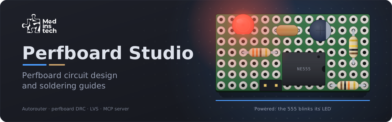
A desktop app where you draw a circuit, lay it out on perfboard — or on stripboard,
or on a solderless breadboard first — let the router work out the connections, prove
the board matches the schematic, and get a step-by-step build guide with measurement
checkpoints.




Download · uv tool install perfboard-studio · MCP server · Example boards · Changelog · Türkçe
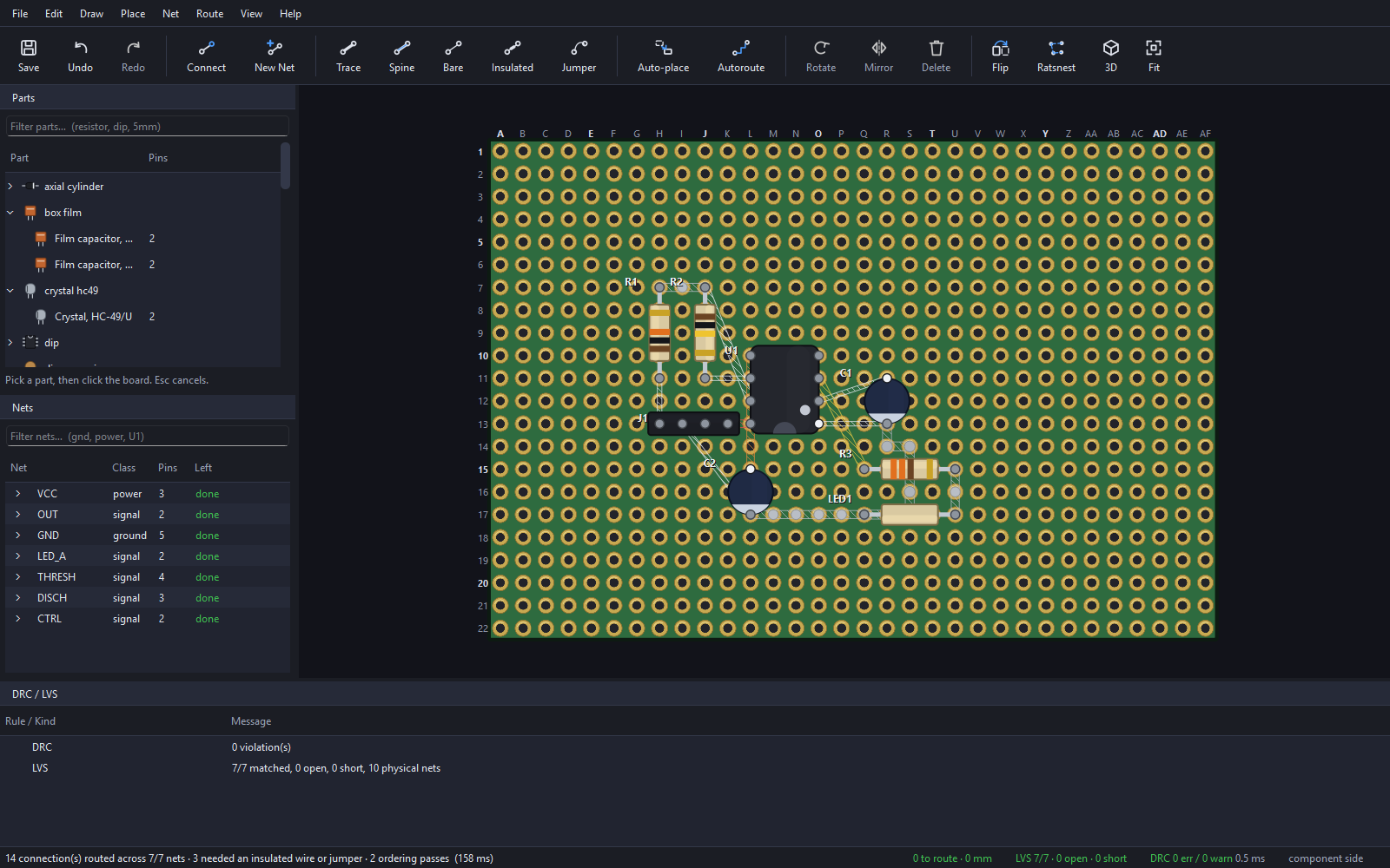
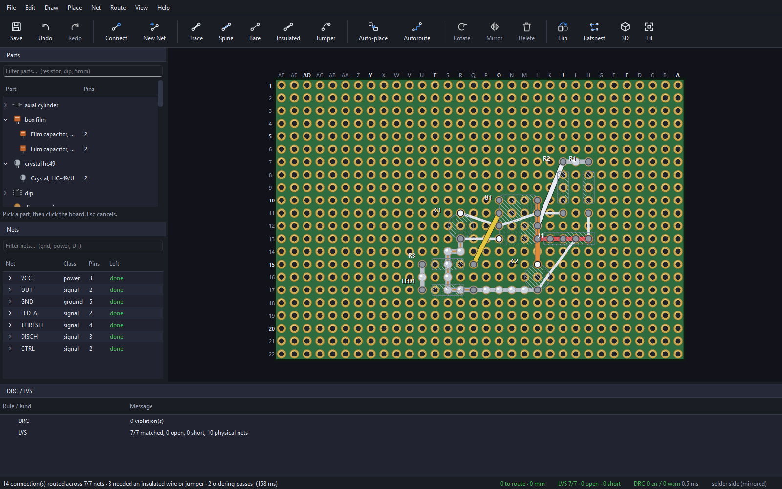
The status bar is the whole claim: fourteen connections across seven nets, no DRC
error and LVS agreeing with the schematic — and one pad to measure for isolation, the
warning below, which the build guide turns into a check with a meter.
- A soldering guide with verification steps. Not just "solder R1 here", but "block 2 complete → U1 pin 4 to C3(−) must show continuity" and "before power-on: GND to V+ must read above 10 kΩ". Derived from the netlist, so it is exact rather than generic advice.
- Perfboard LVS. The board's real connectivity is extracted and compared against the schematic. Opens, shorts and floating conductors are reported before you pick up the iron.
- Six kinds of connection, not one. A lead bend, a solder trace, a wired solder trace, bare wire, insulated wire and a top jumper have different costs, limits and failure modes, and the router prices all six — which is what makes a layout that is pleasant to actually solder.
- A breadboard first, then the perfboard. A solderless breadboard is a board type too: placed, wired with jumpers and power down the rails, and given a building guide with no iron in it. When the circuit works, the same design goes on to perfboard.
- Three rules only the third dimension can see. A part too tall for the case, a jumper trapped under a body that gets soldered down on top of it, and a heat-sensitive part sitting too close to a hot one. The 3D view is a checking tool, not a picture — and the board leaves as a STEP model of the same bodies, to draw its case round.
- Real parts, by name. Pick a BC547, a 7805 or an Arduino Nano out of the catalog and it arrives with what its datasheet calls every lead. A KiCad netlist, if you have one, comes in the same way — and where its symbol numbers the pins differently from the part in your hand, they are renumbered by name, so the board is wired for the part you actually solder.
- Agent-native. An MCP server, a headless CLI and a git-diffable project file, all driving the same command bus as the GUI — so undo works across a session where a human and a model both edit the board.
Status: pre-alpha, and end to end. A circuit goes in and a soldering guide comes out. What is missing is the dogfood test — nobody has yet built a real board by following a generated guide, and PLAN.md §11 says M5 does not close until somebody has. Everything else runs, and every release ships an installer for each of the three desktop platforms, none code-signed.
Jump to — Running it · Connections · Both faces · Real parts · The schematic · The guide · From an agent · How it is built · Documentation · Contributing
Connections are not all the same thing
Most tools model a perfboard connection as "a wire". Perfboard has six physically distinct ways to join two points, each with its own cost, limits and failure modes — and modelling that difference is what lets the router produce a layout that is pleasant to actually solder:
| what it is | notes | |
|---|---|---|
| lead bend | a component leg bent to a nearby hole | effectively free, 3–4 holes |
| solder trace | adjacent pads joined with solder alone | orthogonal only; ~0.6 mm to the next pad |
| solder trace, wired | the same, over a tinned-wire spine | ~10× lower resistance, no length limit |
| bare wire | tinned wire on the solder side | cannot cross another bare conductor |
| insulated wire | may cross freely | costs preparation time |
| top jumper | insulated jumper over the component side | visible, occupies body space |
The 0.6 mm gap to the neighbouring pad is why solder traces are both so useful and so easy to get wrong. Perfboard Studio scores that risk into the router's cost function, and turns every flagged spot into a measurement step in the build guide.
Or no solder at all. A solderless breadboard is a board type too, in the three sizes it
is sold in, and its holes are named the way it prints them — e12, row letter first. The
placer keeps two nets out of one clip and puts each chip across the groove, the router runs
jumpers into free holes and ground and power down the rails, and the guide becomes a
building guide: jumpers first, flat on the plastic, and no iron anywhere. When the circuit
works, File ▸ New Board from This Design takes it on to perfboard, and the breadboard's
file stays as it was.
Both faces, and the third dimension
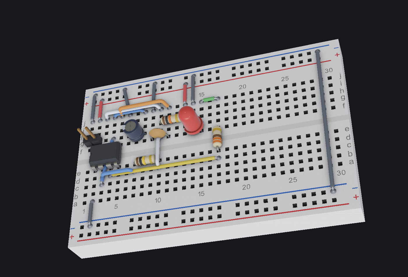
The solder side is where the copper is, so it is a first-class view rather than a mirror mode — and copper on the face you are not looking at is hatched, because a board is opaque and a trace drawn solid says this is in front of you.
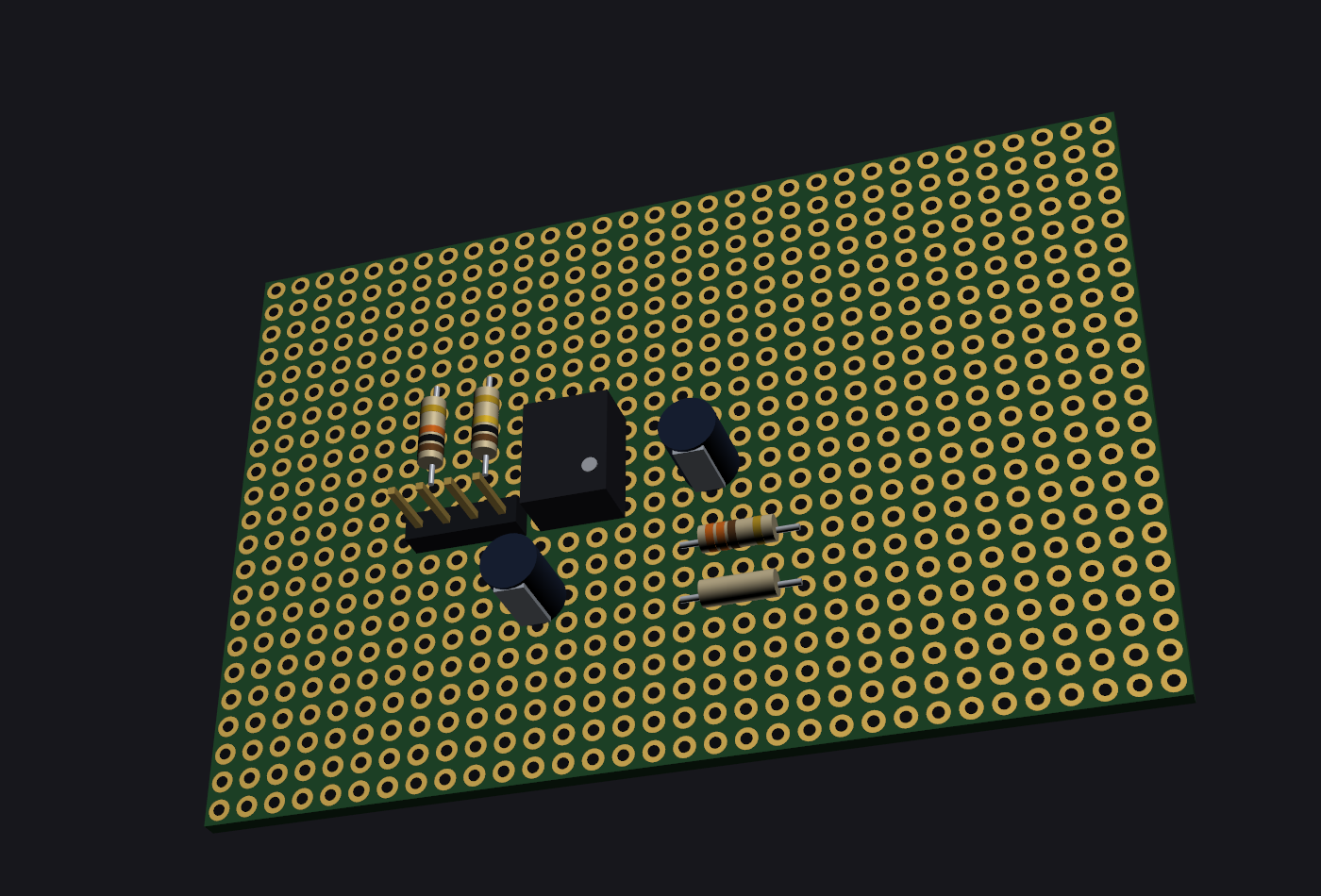
The 3D view is a checking tool, not a picture. Three rules exist that a top-down view cannot see at all: a part too tall for the case, a jumper trapped under a body that will be soldered down on top of it, and a heat-sensitive part sitting too close to a hot one.
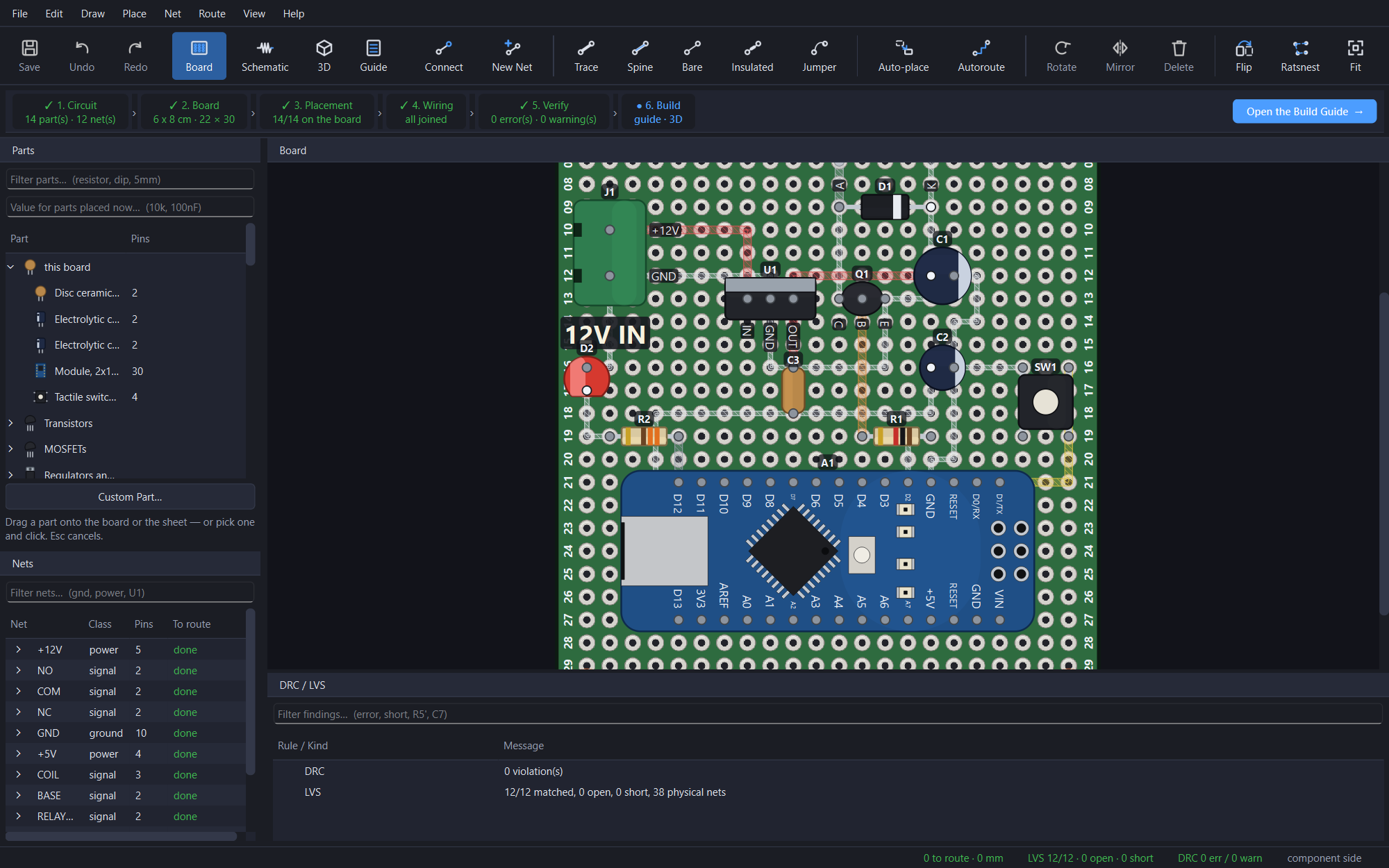
It stands beside the board, and it answers a click. Board, schematic and 3D open side by side, each taking its share of the window, and the toolbar's view buttons switch them on and off. A part clicked in 3D is selected on the board and on the sheet, and the build guide goes to its step; a wire clicked there lights its net everywhere; and whatever is selected anywhere is tinted in 3D, so the three views show one selection.
And it leaves as STEP. File ▸ Export 3D Model (STEP)… writes the board as solids a mechanical CAD program can measure and cut a box round: the board with every hole and mounting bore through it, each part as the room it takes — the very outline and height DRC's overhang and too-tall rules measure — every lead down through its hole, and every wire as thick as the gauge the cut list prints, lifted over whatever it crosses. The application writes the file itself, so it needs no graphics driver and no extra dependency, and a project save puts one beside the other outputs.
Real parts, by name
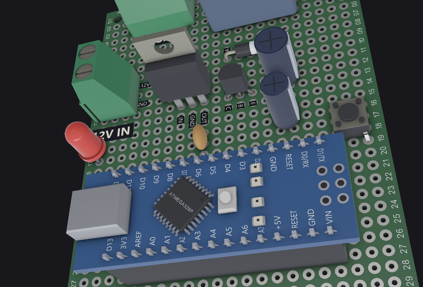
A package is not a part. A TO-92 is a BC547 or a 2N7000 or a 78L05, and which leg is the base is the fact the board depends on. The Parts panel starts with a catalog of the parts a perfboard is actually built from — transistors and MOSFETs, regulators, diodes, DIP ICs, push buttons and dev boards — and picking one places it with its value, what its datasheet calls every lead and the symbol it is drawn as, each with the datasheet it came from.
Those names are printed beside the pins, on the board and in 3D, because a terminal or a devkit is wired by them. They are laid out for the whole board at once: a name stops at whatever is in its way, a part in one row prints its names on its clear side, a name short of room is narrowed, and one with none is left off and listed in the part's tooltip. A dev board is a module — its own board standing on its header strips — drawn as what is on it, in both views, measured from the makers' drawings and KiCad's models: a Nano's chip turned on its corner, its USB socket and its reset button; an ESP32 devkit's radio can and antenna; a Pico in green. Which way round it goes is plain from the picture. And the board can be written on: a label such as "12V IN" beside the terminal that takes it goes on either face and is printed on the 1:1 sheet and in the guide.
A KiCad netlist comes in as parts, not guesses. The board above is
examples/nano-relay.net imported as it stands. Its values
name catalog parts — the Nano, the BC547, the 1N4007, the 7805 — and its KiCad footprint
names measure the rest, from R_Axial_DIN0207_L6.3mm_D2.5mm_P7.62mm to SW_PUSH_6mm. The
pins are renumbered by name where the schematic's symbol numbers them differently from the
part: KiCad numbers a Nano down one side and up the other, its LED cathode first, and a
generic transistor symbol with "BC547" typed on it emitter first — each of which, taken at
its number, would wire the board for a part that does not exist.
A part on the panel is wired, not placed. A pot, a jack or a footswitch that lives in the enclosure goes onto the panel from its right-click menu: on the board it becomes the row of pads its wires land in, where its pins were, so the copper still reaches them, and on the sheet and in the parts list it is still a pot. The guide wires it in with the long wires, says which pad goes to which lug and over which edge the wires leave, puts every wire on the cut list in its net's colour, and checks its nets only once its wires are in.
Draw the circuit first
The board says where everything goes. The schematic panel (Ctrl+2), which opens beside
it, says what you are building — and it is where you say it: Add Part, Wire two
pins, Place on the Board. The circuit comes first and the layout second, which is how
every other EDA tool works and is the order this one could not do until now.
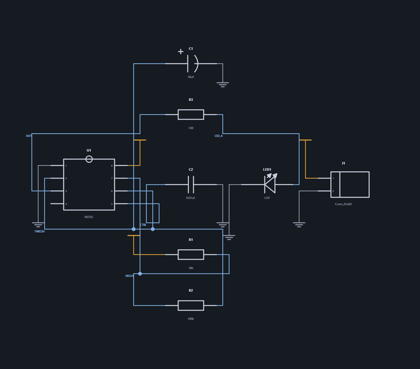
The sheet is laid out for you until you take it over. Until anything on it is moved it is drawn from the netlist, so there is nothing to keep in step; move a symbol, turn one or draw a wire, and from then on the sheet is yours. A wire goes from pin to pin, or onto a wire already drawn — a T, with a dot where it lands — and a net too busy to draw is joined by name with a label at the pin. Ground and power become rail symbols instead of wires, which is the difference between a sheet you can read and eleven lines crossing everything. Polarity comes from the parts library's own pin names, so an LED's cathode and a diode's cathode both end up on the barred end — they are opposite pins, and a rule that guessed from pin 1 would draw one of them backwards. A part whose pinout the library does not record, like a TO-92, is a labelled box: drawing a transistor there would be asserting which lead is the base.
It also cross-probes: click a symbol and that part is selected on the board, click a wire and its net lights up in both places. LVS saying net VOUT is open is a great deal more useful when you can look at VOUT.
And it leaves the window. File ▸ Export Schematic… writes the sheet beside the document three ways: SVG to embed or edit, PDF to print and keep next to the board, PNG to paste into the message that asks somebody why the circuit does not work. All three come out of the same SVG, so they cannot disagree about what the circuit is — and the exported sheet is black on white rather than the panel's light-on-dark, because the rail symbols already say which rail sinks and which sources, and a photocopier keeps shapes rather than colours.
The guide has an order, and you can watch it
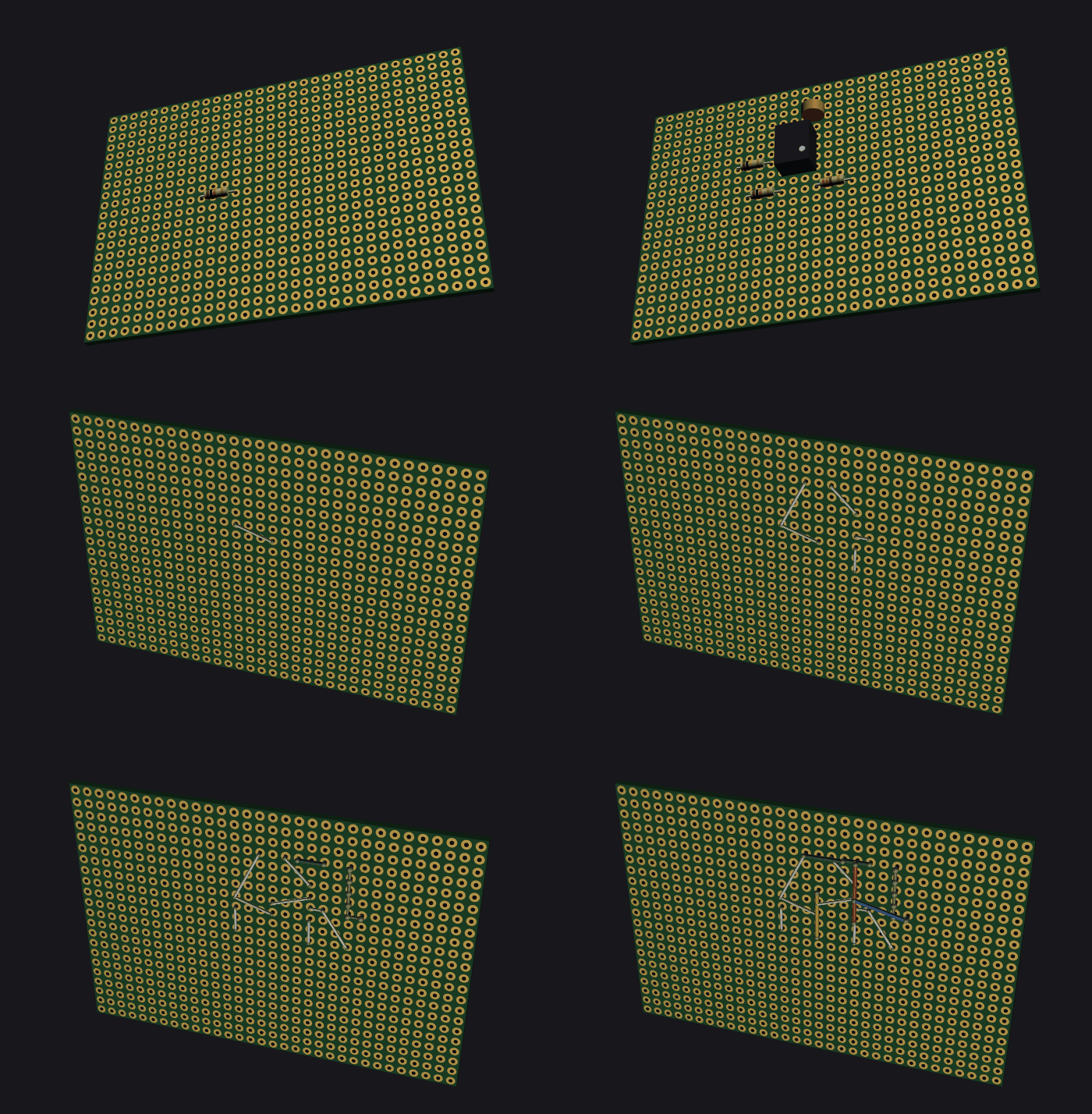
Parts go in shortest first — a tall part fitted early stops the board lying flat on the bench while the short ones are soldered. Then the board is turned over and the copper goes on, and ICs are last for heat and ESD. A jumper that would end up trapped under a part body is moved to the first phase, because by the time that part is down it is too late.
The animation turns the board over halfway through for the same reason you would: a perfboard is opaque, and fourteen of this build's twenty-two steps happen on the face you cannot see from above. It is generated by playing the guide back through the same function the 3D panel's assembly slider calls, so it cannot show an order the guide does not actually give you.
Every wire step draws the wire itself twice: bent to its shape over the board's holes, and straight, with every mark measured from one tip. The guide ends with all of them at real size beside a 50 mm ruler — print at 100 %, cut each wire to its drawing, mark it, bend it. Tip to tip a drawing is exactly the length the cut list gives, because both come from the same numbers.
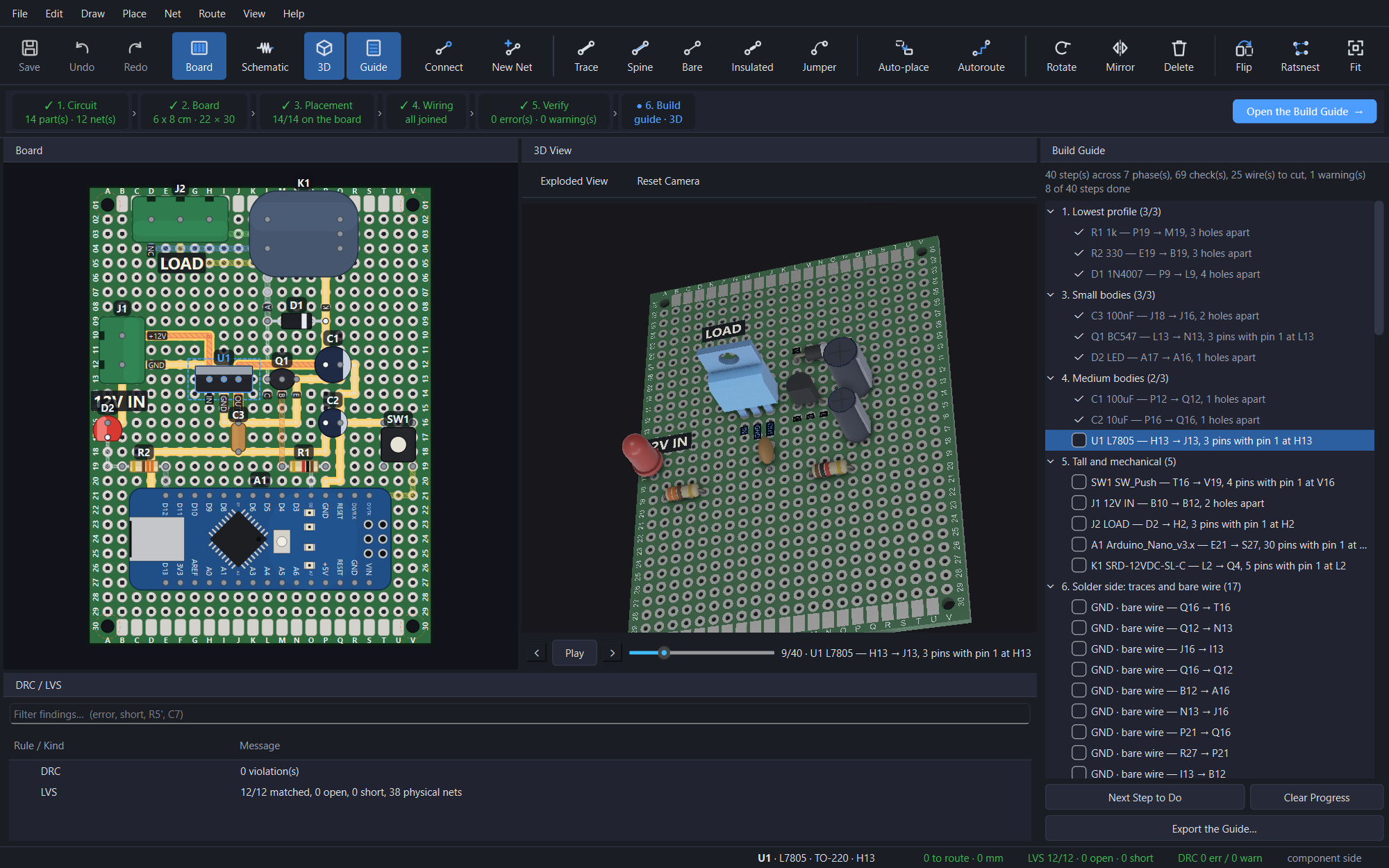
And it keeps your place at the bench. The Build Guide panel (Ctrl+4) stands beside
the board and the 3D view. Tick a step off and it stays ticked for that board — kept in the
application's settings rather than in the file, so ticking is not an edit and joins no undo
— and Next Step to Do picks the first step without a tick: its part selected on the
board, picked out in 3D, and the 3D view showing the board as it stands at that moment of
the build. The arrows either side of Play go one step at a time, which is how somebody
with an iron in their hand wants to move through it.
Running it
It is a desktop application, so the ordinary way to get it is to install one. No Python required.
| Windows | an .exe installer |
| macOS | a .dmg, Apple silicon |
| Linux | an .AppImage, x86_64 |
Each is built and smoke-tested by the tag that produced it. None of them is code-signed, so each warns on first run and the release notes say how to get past it — a Windows EV certificate is ~$300/year and Apple notarization $99/year, and neither is bought yet. See docs/RELEASING.md.
The interface speaks English and Turkish (--lang tr, or follow the system locale),
and so does the build guide it writes — the steps, the checks, the cut list.
From PyPI
For the two platforms with no build — an Intel Mac, Linux on ARM — and for anyone who would rather not click past a signing warning. Needs Python 3.12+:
uv tool install perfboard-studio    # or: pipx install perfboard-studio

perfboard-studio                    # launch on a blank board
perfboard-studio some/board.perf    # ...or open a document
perfboard-studio --version
uv tool or pipx, not a bare pip install, because this is an application and not
a library. Both put it in an environment of its own and perfboard-studio on your PATH, where
pip install would either put 400 MB of Qt and VTK into a shared site-packages or, on
Debian, Ubuntu and Fedora, be refused outright by the system Python (PEP 668). From a
clone, pip install -e . inside a virtualenv.
Qt and VTK are most of that 400 MB. There is no smaller build, because the 3D view is a checking tool the application depends on rather than an optional extra.
A board from nothing
The bar under the toolbar walks through it — Circuit, Board, Placement, Wiring, Check, Build — says where the board stands on each step, and its Next button does whichever comes next. By hand, it goes like this.
Open the schematic panel (Ctrl+2) and draw the circuit: drag parts onto the sheet out
of the Parts panel, move and turn them where you want them, Wire from pin to pin or
onto a wire already drawn (click both ends, or drag) — or Label a pin to join it to a
net by name, or right-click it for GND and +5V — then Place on the Board, which first
asks which stock board to use: your circuit is placed, wired and checked on a roomy board
and on each smaller one, and the suggestion is the smallest it builds as well on. From there
Place → Auto-place Board (Ctrl+Shift+A), Ctrl+R to route, and
File → Export Build Guide (Ctrl+B). No KiCad anywhere in that.
With a circuit that already exists, start at File → Import KiCad Netlist on
examples/ne555-astable.net instead: each part arrives in the design as what its value and
its KiCad footprint say it is, and the step bar across the top of the window takes it from
there — Choose a Board, Place on the Board, route, check, build. That is the
sequence the screenshots above come out of — see
tools/screenshots.py.
Or open one that is already built
Six examples ship as both the netlist and the finished board:
perfboard-studio examples/lm317-supply.perf
| what it is there to show | |
|---|---|
ne555-astable |
the starting point — a 555 flashing an LED |
lm317-supply |
a TO-220 regulator, so the heat rule has something to measure |
lpb1-booster |
built on FR-2, the phenolic board whose pads lift |
arduino-io-shield |
two headers, which is what a shield mostly is |
atmega328-relay |
scale: twenty-four parts, and every rule at once |
nano-relay |
real parts from a KiCad netlist — a Nano on header strips, the catalog's BC547 and 7805, names on the pins, labels on the board |
All six route to completion, match their schematics under LVS and carry no DRC error —
tests/test_examples.py asserts it on every commit.
From an agent
The MCP server drives the identical command bus, so undo works across both:
claude mcp add perfboard-studio -- uvx --from "perfboard-studio[mcp]" perfboard-studio-mcp
Nothing has to be installed first — uvx fetches the package into its own cache. From a
clone it is pip install -e ".[mcp]" and then claude mcp add perfboard-studio -- perfboard-studio-mcp.
Fifty-four tools, every hole addressed the way people talk about perfboard (A1, C7,
AC12) — or, on a breadboard, the way it prints them (e12, T+12) — and never as raw
coordinates — down to export_step, which hands the finished board
to the CAD program its case is drawn in. See docs/MCP.md for the tool list,
the JSON config other clients want, and the rest of the setup.
Headless
Renders the board in 2D and 3D and as the 1:1 PDF, writes the schematic as SVG, PDF and PNG, the STEP model and the build guide, runs DRC and LVS and prints timings, with no display. It is how the visual output is exercised in CI, and the fastest way to check that a rendering change did not crash:
python -m perfboard_studio.ui.main --headless tools/diffcheck/golden/dense.perf
How it is built
The document is immutable and every mutation is a command dispatched through one
bus — which is what makes undo work across a mixed human/agent session. The engine is
pure: no clock, no RNG, no filesystem, no Qt or VTK below ui/. The placer's
annealing is seeded, so the same document and the same seed give the same board.
That purity is load-bearing rather than decorative. This Python engine is a port of the
TypeScript one still in packages/, and its acceptance criterion was never "the tests
pass" but "it produces byte-identical results to the implementation it replaces" —
golden fixtures in tools/diffcheck/, down to the last IEEE-754 double.
src/perfboard_studio/            the engine: document model, command bus, connectivity,
                           router, autorouter, placer, DRC, LVS, persistence
src/perfboard_studio/guide.py    the soldering guide, and guide_export.py for HTML/CSV/JSON
src/perfboard_studio/schematic.py  the sheet, drawn from the netlist until somebody draws it,
                           and schematic_export.py for the SVG the PDF and PNG come from
src/perfboard_studio/boardfit.py which stock board to buy, by building the design on each
src/perfboard_studio/step_export.py  the board as STEP solids, the bodies DRC measured
src/perfboard_studio/stripboard.py  the board whose copper arrives joined, and striproute.py
                           for the cuts-and-links planner that designs on one
src/perfboard_studio/breadboard.py  the solderless breadboard's fixed pattern, and breadroute.py
                           for the jumpers and rails that wire one
src/perfboard_studio/parsers/    KiCad netlist importer, and kicad_parts.py: which part each
                           component is, and which of its legs is which
src/perfboard_studio/ui/         Qt application: 2D editor, VTK 3D view, 1:1 PDF export,
                           and headless.py, the no-display run CI checks the output with
src/perfboard_studio/mcp/        the MCP server (docs/MCP.md)
src/perfboard_studio/catalog.py  the real parts, by name, each with its datasheet
examples/                  netlists to import, and the boards they become
tests/                     ~4250 tests; the engine is mypy --strict clean
packages/                  the original TypeScript engine, kept as the reference the
                           Python port is proved against
The 61 THT footprints are generated from numeric parameters, not shipped as assets. The same spec that draws a part in 2D extrudes its body in 3D, so the two cannot disagree, and a part nobody has a model for is still a whole part.
The 3D view borrows the real shape of the packages KiCad has one for — a TO-220 with its tab and bolt hole, a TO-92 with its legs bent out to the grid, a screw terminal with slots in its screws — because a potentiometer generated from a diameter and a height is a disc with a peg on it. Only the shape above the board is borrowed: the leads through the holes are drawn from your board's thickness, the body keeps its colour from this project's own table, and every part without a model draws exactly as it did. Those meshes are the one part of this repository that is not Apache-2.0 — see Licence.
A part that is not among the 61 is described, not installed. Custom Part… asks for a
pin grid and three dimensions and hands back an identifier that carries them:
box-4x2-p1-r3-15x10x8 is a four-by-two pin grid, three holes between the rows, in a
15 × 10 × 8 mm body. Nothing is stored — the identifier is the definition — so a board
using a part nobody else has still opens as that part on their machine, with no library to
install and nothing to go missing. A surface-mount chip is described the same way:
adp-soic-8 is a SOIC-8 on a DIP adapter, numbered as the DIP-8 it stands in for, and a
KiCad netlist's SOIC, SSOP, TSSOP and MSOP footprints arrive as one.
Where it is going
Done: the editor, the library, connectivity and LVS, DRC, the router and the placement
optimiser, the stock board chosen by building the design on it, the build guide with
rendered step images, 1:1 wire drawings, assembly playback and your place in it kept, the
1:1 PDF export, the board as a STEP model to draw its enclosure round, the schematic panel
with T's and labels and the sheet export beside it, board, schematic and 3D side by side
with one selection between them, a catalog of real parts with their pin names printed on
the board, modules on header strips drawn as what is on them, labels written on the board,
KiCad netlists read part by part, parts described by their own measurements when the
library does not have them, parts on the panel wired to the board, solderless breadboards —
the circuit tried on one and then taken to perfboard —, crash recovery, the MCP server, TR/EN localisation, the
three-platform packaging that a v* tag runs, and the update check that tells you a release exists and fetches it (Help ▸ Check
for Updates; it verifies the download against the release's SHA256SUMS and then hands
it to you — running it stays your click).
Next, in the order PLAN.md §11 puts them:
- The dogfood build (M5). Somebody has to solder a real board from a generated guide. Until that has happened, every claim on this page is a claim about software rather than about a working circuit. It is also the one thing on this list that a stranger can do for the project — there is an issue template for it.
- Code signing. A Windows EV certificate is ~$300/year and Apple notarization $99/year, so until then the installers warn on first run and the release notes say how to get past it.
Where everything else is written down
| docs/MCP.md | the 54 MCP tools, grouped with the reason each one exists, and the client config for Claude Code, Claude Desktop, Cursor and Antigravity |
| examples/README.md | what each example board is there to demonstrate |
| CHANGELOG.md | every release, and what an unreleased build is accumulating towards the next one |
| docs/RELEASING.md | the tag ritual, and what release.yml builds out of it on three platforms |
| docs/prior-art.md | the tools that already exist in this space, and the licence boundary this project keeps from them |
| CONTRIBUTING.md | running the suite, which checks are gates and which are reports |
| SECURITY.md · CODE_OF_CONDUCT.md | reporting a vulnerability, and how people are expected to behave here |
| PLAN.md | the project plan, written in Turkish: what is to be done and what is deliberately not. It is not frozen; it changes when the plan does, and a prediction that did not hold stays where it was with a sentence saying what happened |
| CLAUDE.md | why the code is shaped the way it is. Written for agents working in the repository, and the most useful thing here for a person about to change something |
Contributing
Issues and pull requests are welcome. Please read CONTRIBUTING.md first — it covers how to run the suite, which checks are gates and which are not, and one licence boundary that matters more here than in most projects: do not read or port code from the GPL-licensed tools in this space. Perfboard Studio is clean-room with respect to them, and that has to stay true. The record is in docs/prior-art.md.
Licence
The code is Apache-2.0. See LICENSE and NOTICE.
The 3D package meshes in src/perfboard_studio/ui/models/ are CC-BY-SA 4.0, because
they are derived from the KiCad packages3D library.
They are the only part of this distribution that is not Apache-2.0, and they carry their
own LICENSE
and NOTICE.md
in that directory.
Two questions people actually have:
- Does this affect a board I design? No. KiCad's licence has an exception for exactly
this: designs made with the library, and files generated from them, are not covered. Your
.perf, your schematic, your build guide and the board on your bench are yours, on whatever terms you like. It is the same position as anybody using KiCad itself. - Does it affect a fork, or a build I ship? Only that directory, and only in the usual
CC-BY-SA way: keep its
LICENSEandNOTICE.mdwith it. The rest of the tree stays Apache-2.0.tools/import_kicad_models.pyregenerates the meshes from a KiCad installation if you would rather build them yourself, and deleting them costs nothing but the shapes — every part falls back to its generated body.
1 maintainer

Metadata
1 maintainer
Release files for perfboard-studio 0.19.0
For a detailed explanation of source distributions (sdists) and built distributions (wheels), please see the package formats documentation.
Source distribution (sdist)
| File | Size | Uploaded | |
|---|---|---|---|
| perfboard_studio-0.19.0.tar.gz | 2.2 MB | Details |
Built distribution (wheel)
| File | Interpreter | ABI | Platform | Reset |
|---|---|---|---|---|
| perfboard_studio-0.19.0-py3-none-any.whl | Python 3 | none | any | Details |
Total release size: 4.0 MB
Release files / perfboard_studio-0.19.0.tar.gz
| Download URL | perfboard_studio-0.19.0.tar.gz |
|---|---|
| Size | 2.2 MB |
| Tags | Source |
|
SHA-256 checksum How to use checksums |
c74ed450ddf632467b258786886c3ee7c9ead89b8c6b0639400b6a4ef658a4c2
|
|
BLAKE2b-256 checksum How to use checksums |
62e6694eca4aefd3a6e6b5dfb3ff6ed357bebd11122aa2ac97670ca9e401a9b8
|
| Upload date | |
|
Uploaded using Trusted Publishing? What is trusted publishing? |
Yes |
| Uploaded via |
twine/7.0.0 CPython/3.13.14
|
Provenance
Provenance describes where a file came from. On PyPI, provenance is shared via attestations, which provide a verifiable record of the build or publishing details. View details, limitations and caveats.


PyPI Publish Attestation
PyPI verified that this artifact, at this checksum, originated from the publisher listed below.
Signed by GitHub Actions, verified by PyPI on Oct 16, 2026.
Transparency logRelease files / perfboard_studio-0.19.0-py3-none-any.whl
| Download URL | perfboard_studio-0.19.0-py3-none-any.whl |
|---|---|
| Size | 1.8 MB |
| Tags | Python 3 |
|
SHA-256 checksum How to use checksums |
a6c19b4747f82c20de7d6e83269cd3007840d09ea4e9929a2e903d16c8bf39c9
|
|
BLAKE2b-256 checksum How to use checksums |
e2572dbf182a4c442b4af0a5a106dcf25d6c5e5a954feb5c91523d001790080a
|
| Upload date | |
|
Uploaded using Trusted Publishing? What is trusted publishing? |
Yes |
| Uploaded via |
twine/7.0.0 CPython/3.13.14
|
Provenance
Provenance describes where a file came from. On PyPI, provenance is shared via attestations, which provide a verifiable record of the build or publishing details. View details, limitations and caveats.
PyPI Publish Attestation
PyPI verified that this artifact, at this checksum, originated from the publisher listed below.
Signed by GitHub Actions, verified by PyPI on Oct 16, 2026.
Transparency log