Create AWS Palace FEM Models from GDSII layout files
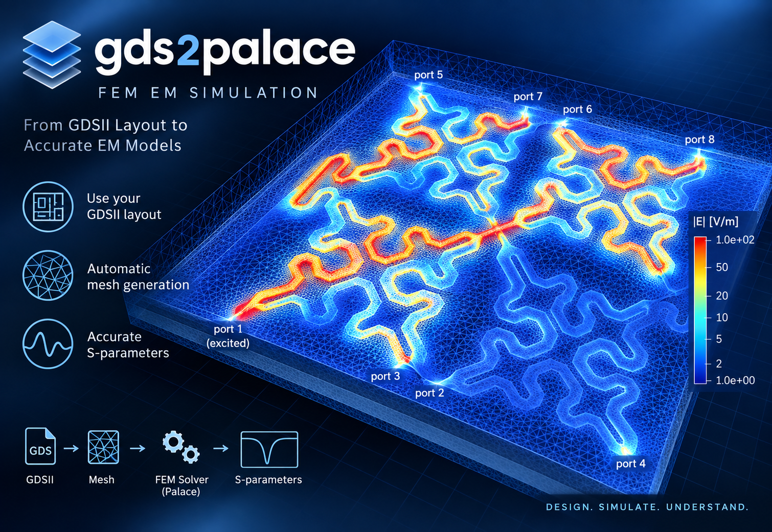
The files provided here enable RFIC FEM simulation using AWS Palace from GDSII layouts created in IHP SG13G2 RFIC technology.
Palace, is an open-source, parallel finite element code for full-wave 3D electromagnetic simulations. It can be scaled from single computer to large high performance simulation clusters and cloud-based computing.
https://awslabs.github.io/palace/stable/
In addition to AWS Palace, gds2palace can also generate models for Elmer FEM, as an additional workflow option for EM (S-parameter) simulation as well as steady-state thermal simulation. See CHANGES.md for this and other recent additions.
The gds2palace workflow in this repository is pre-configured for GDSII layout files in the IHP SG13G2 Open PDK. Special thanks to IHP and the public funded German project FMD-QNC (16ME0831) https://www.elektronikforschung.de/projekte/fmd-qnc for financial support, which has contributed to this work.
Install
pip install gds2palace
Full documentation, installation guide, and usage walkthrough: https://github.com/VolkerMuehlhaus/gds2palace_ihp_sg13g2
Recent changes
11 November-2026
gds2palace 0.10.1
New features
settings['wall_extension']: a dictionary per side, e.g. {'xmax': 2000}, for a side that is not a port wall. The layout's cross-section at that edge (every metal layer that reaches it, no vias) is continued outward by the length, so that the wall sits there. Written by setupEM for the pieces of a split region: where the region has a port wall with a port_wall_extension, a piece without a port on that side gets the same box as the piece with the port.
Port walls with several lines: D (and with it the gap and the standards' length) is that of the largest group of coupled lines, not of the whole span of the lines on the wall. Neighbouring lines closer than twice their distance to ground form a group; a differential pair is one group, as before. A cut across the 8 resonator arms of a PCB hairpin filter (lines 1 mm wide, 0.45 mm above the plane, spread over 17.5 mm) had D = 18.4 mm, 74 mm standards and a calibration valid to 1.1 GHz; now D = 3.4 mm and valid to 3.5 GHz, and the joined pieces agree with the full model. Checked against D per line for a PCB pair over a plane and an on-chip GSSG pair (port_wall_cluster_study, 2026-11-11).
Fix
A via port drawn in the plane of a PEC wall (boundary 'PEC', no dielectric oversize and no air on that side) is shorted by the wall; the result showed nearly total reflection, with no message. The model is no longer written: the error names the port and the side (make the side a port wall, move the wall away, or use another boundary).
Port walls: with a port_wall_extension on one port wall, the standards of a port wall next to it (around the corner) were wider by the extension on that side, as the model is, but their metal ended at the layout edge. The metal that reaches the extended wall is now continued in the standards' cross-section too, as in the model.
10 November-2026
gds2palace 0.10.0
New features
Calibrated de-embedding of ports at a port wall. A box side set to 'PORTWALL' in settings['boundary'] is a PEC wall right at the layout edge; the ports drawn on that edge, over the ends of the lines, are removed by calibration instead of the estimated port inductance. gds2palace cuts the gap between the wall and each line, and writes two standards per port wall into the model's _data folder: the cross-section at the wall extruded to thru lines of length L and 2 L (L = 4 D, D = span of the lines + 2 x distance to ground), with the model's stackup and mesh settings, at three frequencies. run_sim solves them before the model and reuses unchanged results; combine_extend_snp.py removes the port and the coupling between the ports on the wall (double delay) and writes one comment line per port into the _deembedded file, plus <model>_deembedding.json with the port elements, the line at the wall and warnings. New settings reference_plane_shift, deembedding_length, port_wall_extension (move the port wall outward by 'auto' or a length: the feed is extended by the cross-section at the wall and the reference plane shifted back to the layout edge, for a device close to the wall) and deembedding = 'none'. A via port on a port wall (e.g. from the KLayout plug-in's export) is used as a gap port on its line's metal, when one end is the line and the other is not; otherwise the model is not written. The cross-section must stay the same for D/4 into the layout only within D of the lines, and only without a port wall extension that gives that straight length (with one, metal close to the layout edge is accepted, and the warning that the wall mirrors the device is left out); the check finds a change exactly, also a feature narrower than its D/8 sampling grid (it samples just past every polygon vertex); metal farther away that changes near the wall (a slot in a plane that closes, a pad frame ending) is only noted; on a line over a Metal1 plane (D = 30 µm) such a change gave differences below the mesh noise (test_data/port_deembedding_study/far_change, 2026-11-08). Without a port wall, models are unchanged. Every model's _data folder now also holds combine_extend_snp.py, the result script of the gds2palace that wrote the model, and scripts/combine_snp (and the Linux installer's wrapper) runs that copy when present: the Touchstone conversion and the de-embedding match the model, whatever copy is installed in ~/scripts; run_sim warns about a wrapper that would not use it, and the script prints its version first. Update your combine_snp once from scripts/. The rules come from test_data/port_deembedding_study; see "Calibrated de-embedding at port walls" in the user guide. First automated tests of gds2palace: python -m pytest tests.
settings['margin'] can be set per side: a single value (all sides, as before) or a list of 4 values [margin_xmin, margin_xmax, margin_ymin, margin_ymax]. Without air_around, the air then follows the margin of each side, and zmin and zmax use the largest margin. Models with a single value are unchanged. A negative margin now stops with an error: it cut the dielectrics smaller than the drawing without notice. A conductor, via or sheet layer that reaches an absorbing boundary now gives a warning, because the boundary changes its result.
Stackups (XML_stackup/latest/IHP): two target layers for heat sources, HEAT_TRANSISTOR (the top 40 nm of Activ, silicon) and HEAT_RESISTOR (a 0.16 µm polysilicon body with 20 W/m·K above the Activ level, i.e. on the field oxide). A heat source takes the z range and the material of its target layer, and nothing is drawn on the two GDS layers (320, 321), so EM models are unchanged. With Activ as the target, a transistor's heat source was ten times too thick and a resistor's heat source was silicon on the substrate; both came out too cool. At a heat source mesh of 0.125 µm, an npn13G2 with 8 emitters now has about 1740 K/W instead of 1300 K/W; the converged value is about 1890 K/W (PDK model: 1750 K/W). Resistor results are not validated yet. See "Heat source targets" in XML_stackup/latest/IHP/README.md.
Fix
A conductor that reaches the simulation boundary, with margin and air_around both 0 on that side, stopped Palace with an MFEM abort in STable3D when using the surface conductor model. The conductor's end face belongs to no meshed volume, but was written to the mesh as a boundary. It is now left out; the boundary condition applies to the rest of that side. If that face is the conductor's top or bottom face, the conductor gets "External": true, because its other main face now carries all the current. Other models are unchanged. See "Conductors at the simulation boundary" in the user guide.
Elmer thermal: a heat source that partly overlaps another volume (e.g. a heat source that reaches under a contact) lost its mesh refinement. The model was built and solved with a coarse mesh at that source, and the only sign was the message that its refined_cellsize_override entry is "neither a heat source nor a metal layer". Heat sources inside one volume or in the oxide are unchanged.
A model whose metals are all sheets (zero thickness, e.g. a PEC line on a PEC ground sheet) stopped with the gmsh error "Difference failed - BOPAlgo_AlertTooFewArguments": there was no metal volume to cut out of the dielectrics. The dielectrics are now left as they are in that case. Other models are unchanged.
5 November-2026
gds2palace 0.9.4
New features
util_thermal_map: powers from a circuit simulation onto the heat sources of a thermal export. The thermal export of the KLayout EM Export plug-in puts each transistor and resistor on a heat source layer of its own and writes <name>_thermalmap.json (layer, layout device and, from LVS, the schematic instance name per heat source). read_powers() reads a file with one line per device (instance name and power in W; comma, semicolon, tab or spaces; SPICE suffixes), apply_powers() returns the power per heat source layer and a report of heat sources without a power and names that match no heat source or several. Nothing is set silently. Command line: python -m gds2palace.util_thermal_map <name>_thermalmap.json powers.csv <name>.tsimcfg writes the powers into a setupThermal file. setupThermal's Load powers... uses it.
Elmer thermal: refined_cellsize_override now works for thermal models too. A heat source in the list (source_<GDS layer>, e.g. ['source_205', 0.25]) gets its own mesh size instead of refined_cellsize, e.g. a fine mesh only at the emitter fingers of an npn. A metal layer in the list gets edge refinement at its value, growing to meshsize_max like the mesh around a heat source (below); thermal models refine no metal edges otherwise.
Elmer thermal: the mesh around a heat source now grows at a fixed rate, 0.3 µm per µm of distance, to the maximum size away from the sources. Before, it reached the maximum size within 30 times the source's mesh size, which is very fast for a small mesh size: for an npn13G2 with 0.25 µm at the emitter fingers, the temperature rise came out about 20 % too low. Models whose maximum size is more than 10 times the mesh size at the sources get more elements; at 10 times (e.g. 2 µm / 20 µm) the mesh is the same as before. The thermal example (5 µm / 100 µm) has 98k instead of 74k elements, with the same peak temperature within 0.1 K. Without the setting, thermal meshes are unchanged. Names that are neither a heat source nor a metal layer of the model are reported.
Fix
Elmer thermal: a temperature-dependent thermal conductivity (ThermalConductivityTable, e.g. silicon) was taken at 0 K. The model had a single heat solver iteration and no initial temperature, so Elmer read the table once at 0 K, far below its range, and extrapolated it linearly: about 270 W/m·K for IHP's silicon table instead of 82 W/m·K at 300 K, and about 380 W/m·K for the literature table of the thermal example. Temperatures came out too low. A model with a table now starts at the lowest constant temperature of the model and iterates until converged (at most 50 iterations). The thermal example now gives a temperature rise of 48.0 K instead of 39.7 K. Models with constant thermal conductivities are unchanged.
Stackups (XML_stackup/latest/IHP): Activ's thermal conductivity is now the silicon table Si_vs_T_IHP instead of a constant 50 W/m·K that had no source. The heat sources of a thermal export sit in Activ, so this value decides much of a transistor's temperature rise. Thermal models of devices now come out cooler; EM models are unchanged.
Elmer thermal: a heat source inside a conductor of its target layer (an npn emitter's heat area in Activ) stopped the model with "Polygon on conductor layer source_... touches another conductor layer". The heat source takes the target layer's material, so the face it shares with that conductor is an interior face; it now stays with the conductor's surface group (thermal surface groups are only for viewing, boundary conditions come from the constant-temperature groups). Heat sources outside conductors (resistors over field oxide) are unchanged.
Mesh check: after meshing, elements of zero (or negative) volume are reported with their volume and position. A coarse mesh around small conductors (e.g. 0.7 µm metal fingers with a cell size of several µm) can leave flat tetrahedra in the dielectric between them, which gmsh's optimization keeps; Elmer then stops with "Degenerate 3D element" and a NaN solution. For Elmer models (thermal and EM) this is an error before the mesh is written, with the hint to use a finer mesh (refined_cellsize, meshsize_max); for Palace a warning.
ElmerGrid check: the conversion of the gmsh mesh to an Elmer mesh (and the split for MPI) now stops with an error when ElmerGrid fails. A crashed ElmerGrid (a segmentation fault on a large thermal mesh, on Windows and Linux) went unnoticed until ElmerSolver reported a missing mesh folder. When the ElmerGrid location is unknown (Windows: ELMER_HOME set but empty), the message no longer fails on an undefined variable.
Full history: CHANGES.md
Note: the gds2palace PyPI package itself only requires:
- gdspy>1.6.0
- gmsh
- numpy
- shapely>=2.0
(Other Python modules mentioned above are only needed to run the example/model scripts in this repository, not to use the installed package.)
1 maintainer

Metadata
1 maintainer
Release files for gds2palace 0.10.1
For a detailed explanation of source distributions (sdists) and built distributions (wheels), please see the package formats documentation.
Source distribution (sdist)
| File | Size | Uploaded | Provenance | Actions |
|---|---|---|---|---|
| gds2palace-0.10.1.tar.gz | 170.7 kB | Without provenance | Details for gds2palace-0.10.1.tar.gz |
Built distribution (wheel)
| File | Interpreter | ABI | Platform | Actions Reset |
|---|---|---|---|---|
| gds2palace-0.10.1-py3-none-any.whl | Python 3 | none | any | Details for gds2palace-0.10.1-py3-none-any.whl |
Total release size: 331.6 kB
Release files / gds2palace-0.10.1.tar.gz
| Download URL | gds2palace-0.10.1.tar.gz |
|---|---|
| Size | 170.7 kB |
| Tags | Source |
|
SHA-256 checksum How to use checksums |
08158ce809692e341add3ab7d483de3460cfa6286ec4b572f3996db85bcd9e0e
|
|
BLAKE2b-256 checksum How to use checksums |
9c89de37251be27d661bf72775ca4910b1d38791e8153f662df8cf5e109bb905
|
| Upload date | |
|
Uploaded using Trusted Publishing? What is trusted publishing? |
No |
| Uploaded via |
twine/6.2.0 CPython/3.13.14
|
Release files / gds2palace-0.10.1-py3-none-any.whl
| Download URL | gds2palace-0.10.1-py3-none-any.whl |
|---|---|
| Size | 160.9 kB |
| Tags | Python 3 |
|
SHA-256 checksum How to use checksums |
8337f011d2ab81c31c3ce2807546a04243fc7e4d9897b3f845d564ead8050faf
|
|
BLAKE2b-256 checksum How to use checksums |
12aa154b30d8a008dbd0e8b0b6e215cebec461270f2adee522ebf4c9e769cbaa
|
| Upload date | |
|
Uploaded using Trusted Publishing? What is trusted publishing? |
No |
| Uploaded via |
twine/6.2.0 CPython/3.13.14
|
Security for gds2palace 0.10.1
Provenance
Provenance describes where a file came from. On PyPI, provenance is shared via attestations, which provide a verifiable record of the build or publishing details. View details, limitations and caveats.
No provenance found
None of the files in this release were uploaded with provenance metadata.
A note on package security
PyPI is a repository for distributing packages, not a service for auditing them. While third-party security researchers and our staff do their best to detect and remove malicious packages, PyPI cannot guarantee the quality, security or suitability of any given package.
To learn more about protecting yourself from malicious actors, visit our package security documentation.